Adsorption tests on PEG1000 etc.
I was given three groups of chips to SEM. The first group had undergone the Diazerine and PEG1000 treatment followed by incubation with either PBS, IgG, or BSA. The second ‘group’ was a chip that had been treated with diazerine and PEG1000 but had not been incubated. The last group was a chip which had not been treated at all, to assess whether the pores had changed during the etching processes which happens before the diazarine step.
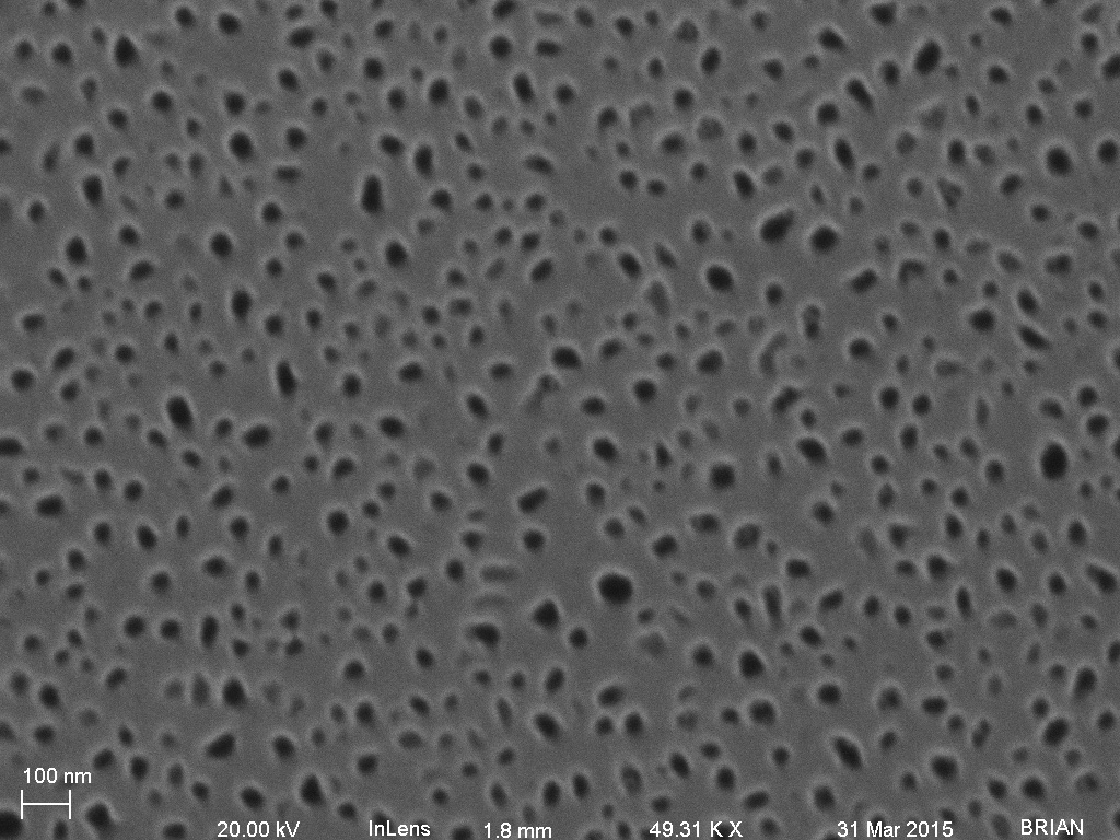
The quality of the SEMs are not very good. I had Brian McIntyre helping me to get the best images possible. Our original thought was that something in the process is causing the surface to charge, either the gold doesn’t adhere or the surface charges anyway, but the first images I show are bare chips straight from the wafer (wafer # 1154) and those aren’t really any better.
Original Untreated clean sample 50,000 x, 100,000 x, 100,000 x
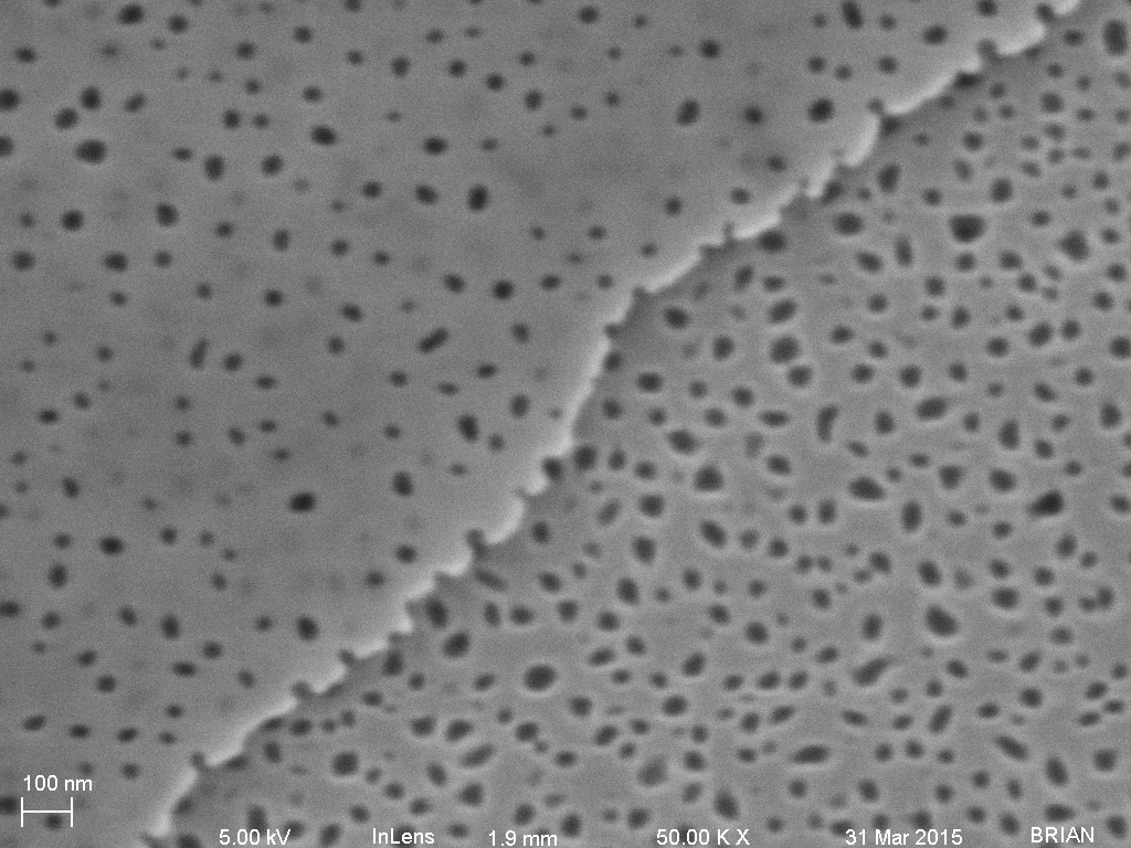
Unprocessed chip, on left compared to PEG 1000 treated (PBS incubated) on right. I didn’t do an analysis but to the naked eye there doesn’t seem to be a significant change in hole size.
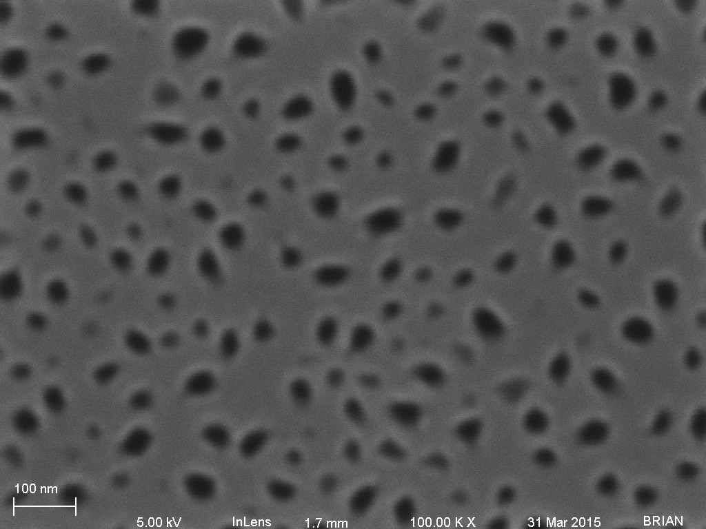
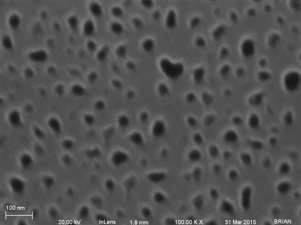
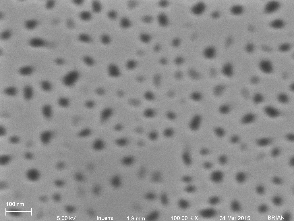
The remaining images have all been PEG 1000 treated
BSA 100,000 x

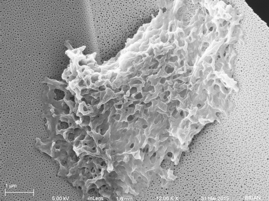
IgG 100,000x, weird clump on IgG 12,000 x
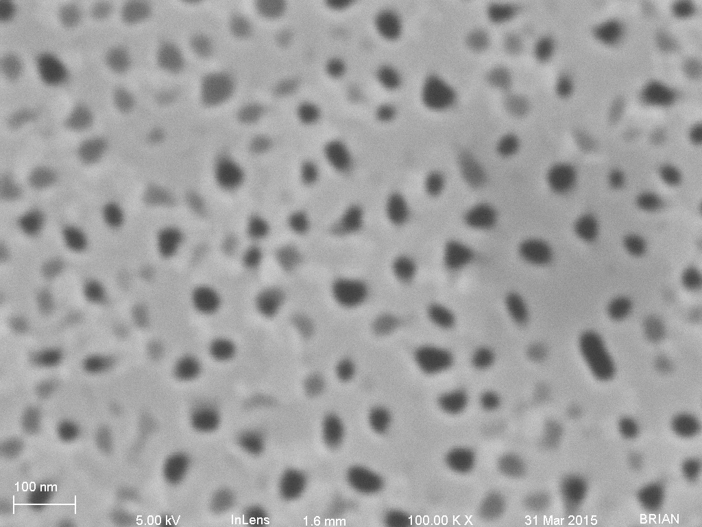
PBS 100,000 x

PEG 1000 only 100,000 x, PEG 1000 only 50,000 showing backside of membrane folded over. This shows more clearly the pits vs true pores.
Please update with BSA pics
Unmodified controls