Nanoporous SiN Lift-Off Update – April 2015
Background Details:
Josh Miller & I have made some recent progress in the NPN LO work. We had several ø6″ wafers w/ 100 nm of thermal oxide processed by Rogue Valley, wherein they deposited 650 nm of poly-Si (LP-CDV) followed by 50 nm of low-stress SiN (LP-CVD). Josh added the a-Si + SiO2 layers at URNano to two of these wafers and ran them through the RTP. He then performed the nanopore transfer into the nitride using RIE in the Trion at SMFL. After a brief strip of any remaining pnc-Si in the Xactix, he deposited ~30 nm of TEOS SiO2 to aid SU-8 adhesion. We spin coated a 10 µm layer of SU-8-3010 and patterned a hexagonal scaffold with 100 µm (flat-flat) openings and 10 µm wide struts. Bob put the wafer in 10:1 BOE w/ surfactant to strip the oxide. We cleaved the wafer into ~1″ x 1″ pieces and tested through-pore etch in the Xactix. We also tested transfer to a 3-D printed hemodialysis module that Josh designed with input from Dean.
High-level Summary: The NPN membrane using the Rogue Valley coatings perform very well in the through-pore etch. We are able to get complete sacrificial layer removal with about six pulses of XeF2 etchant. We also are able to transfer these membranes section successfully to the hemodialysis modules. We are having issues with damage to some of the NPN windows in the lifted-off membranes. We believe this is related to stiction of the membrane to the wafer surface after the window areas have been cleared of the sacrificial poly-Si. We have a number of ideas to pursue to mitigate this issue.
Device Design:
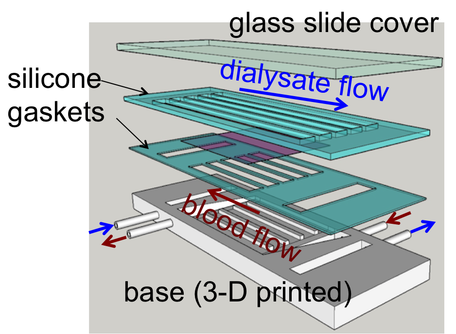
Below is a schematic of the dialyzer module. It’s designed to hold a membrane of ~1″ x 1″. The base is 3-D printed, and the membrane is held between two PDMS gaskets. Separate flow paths for blood and dialysate are defined by the base. A glass slide is used as the top cover. As a side note: the image on the right shows a concept for a mold that could machined (or possibly 3-D printed) that would enable one to create the base part of the module using Sylgard.

Through-pore Etch:
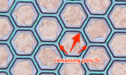
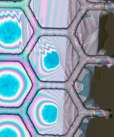
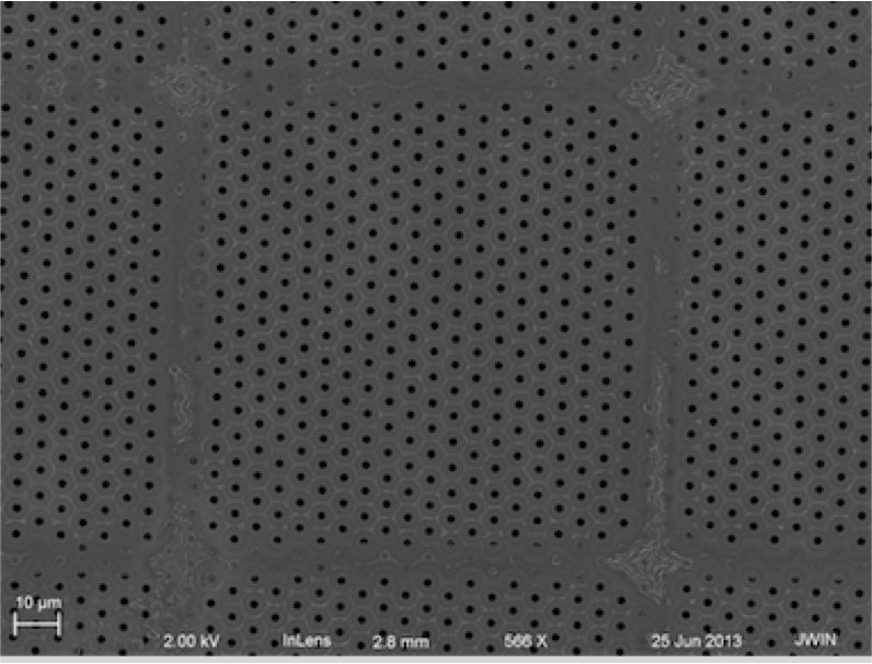
These two micrographs show a NPN membrane that had been exposed to four pulses of XeF2. Nearly all of the sacrificial poly-Si layer has been removed and only small connection points at the intersections of the SU-8 grid remain (see arrows in left-hand image). Also, note that the membrane appears to have “settled” to the surface of the wafer in the windows of the SU-8 grid. The image on the right taken near the edge of the wafer shows a bit of membrane that is curling up and illustrates the contrast of the NPN when it is free of the wafer surface.
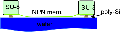
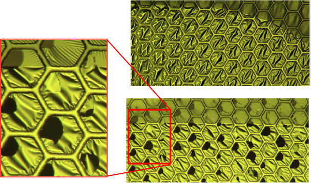
This image below on the left shows a cartoon depiction of what Josh & I believe is happening. The NPN membrane is considerably more flexible at the ~10 µm length scale compared with the microporous SiN. An SEM micrograph of that material is shown below on the right. Note that the open window for the µ-porous membrane (also 50 nm thick) is very flat, so it would appear that the presence of the nanopores makes the membrane much more flexible. Also, note that the µ-porous membrane shows evidence of a residue on the bottom surface of the membrane that we assume is contaminant that was in the poly-Si (deposited in the SMFL for the µ=pores). We haven’t checked the NPN LO samples for this yet, but Josh & I are guessing there will not be a similar residue from the Rogue Valley poly-Si. Ironically, this “crud” may be helpful to LO in that it prevents stiction of the membrane (think of the analogy of dusting a counter with flour prior to rolling out a pie crust). Maybe the Rogue Valley poly-Si is too pristine for our own good?!
Images of Lift-Off Samples
Below is a photo of a sample that had been successfully transferred to the hemodialysis module. When we inspect the membrane under optical microscopy, we find there are regions where SiN windows are torn as seen in the bottom micrograph plus center blow-up below. The top micrograph shows a region where there is no damage. Both regions show the interface of the membrane near the edge of the PDMS gasket. The torn windows appear after lifting the membrane from the surface of the wafer. They are NOT caused by placing the membrane on the PDMS gasket.

Josh thought the stiction-related damage might be mitigated by floating the LO membranes from the wafer surface using water. He placed the sample that had undergone the through-pore etch on a small square of sticky PDMS in a petri dish and slowly filled the dish with DI water. This does result in floating the membrane from the surface of the water as seen in the photo below. Also, this resulted in substantially less damage to the membrane. I haven’t carefully quantified the damage, but nominally, this sample showed a couple of the open windows of the PDMS gasket that had no holes and perhaps just ~20% of the area in the remaining PDMS windows showing tears in the SU-8 windows. In contrast, the dry LO samples show more like ~50-75% damage more uniformly across the whole membrane area.

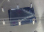
One other issue we found is that as the membrane starts to release from the surface in the Xactix, the edges curl up as seen in the photo below. We believe this must be prevented or the force of the curling membrane will cause damage to the membrane that has stuck to the surface. The curling is caused by the slightly higher tensile stress of the SU-8 layer.
Future Ideas:
The following are our immediate ideas to try, and we would welcome suggestions:
- Try a smaller grid size for the SU-8. We have square grids with both 50 and 75 nm openings.
- Use some porous cover on the sample during the XeF2 etch to prevent the edges from curling. This would have to be transferred to the water float fixture.
- Ask Rogue Valley to add some crud to the poly-Si. OK, this is mostly in jest, but there could be some utility to adding something to this layer that does not get removed. One thought I had was perhaps to expose the sample to air for a few hours after a single XeF2 pulse to create a small amount of native oxide. This would be tricky to calibrate the air soak time such that we get some amount of oxide to mitigate stiction w/o forming too much such that the subsequent LO etch is prohibatively slow. Another potential issue with this approach is that any residue may post a contamination issue for the final application.
- If we can limit the regions of damage to only a couple spots in the ~ 1″ x 1″ sample, these could presumably be later patched by drizzling a little Sylgard over them.
I’m really going to try to make NRG tomorrow to get caught up on recent advances – lots of interesting stuff going on!!
A few quick thoughts on this post:
1. The stress difference between the SU-8 scaffold and the NPN is a big problem that you will be constantly battling. Not only does it cause the annoying curling, but the micro-wrinkles are a big part of your stiction problem. I would focus on developing some way to eliminate this. Easier said than done, I know. Maybe try thermal reflow of the SU-8, swell the SU-8 with toluene and hope it does not completely reverse, stress balance with higher stress SiN, some compensating layer under the SiN, geometric relief of some kind in the scaffold pattern, or maybe replace SU-8 with something else?
2. The stiction problem is made worse by the surface charges on the SiO2. I would think that replacing the SiO2 with SiN would be much better and would not change your process much.
3. Call me a hater, but I do not like any process that involves floating a membrane, especially for lift-off. If you have a dry process that undercuts the membrane, you have a huge head start on a scalable and manufacturable process. Watching this beautiful process setup go into water is like finger nails on a chalkboard to me. Maybe it’s my bad attitude!! 😉
Great progress – hopefully you are well on your way to increasing yields and producing football fields of this stuff, by reusing wafers 100’s of times!! Thanks!