Bonding SiMPore Chips Directly to Glass has been Difficult
Our friends at McGill university have wanted to incorporate our chips directly into their platform for squeezing and confining DNA. Their desires come in a form of a device where we can seal the SiMPore chips into glass channels without any intermediate gasket layers.
In the video above, we can see the relevant layers, a bottom channel that is made of etched glass (green) a top channel that is made of etched glass (gold), with a circular depression and routing fluidics, and a SiMPore chip that has a set of finely patterned grooves (steel) on top of nitride (copper). The idea is to inject DNA solution into the device, then flex the top piece into the coverglass.
Our chips are doubly bondable, but the bonding on either surface may have different requirements. For instance, the bottom bond between the bottom channel and SiMPore chip must be as small as possible to minimize working distances in the device. The top channel bonding layer has to provide fluidic access to the bottom channel and maintain a separate chamber for introducing DNA solution to the device.
We have tried to bond our chips directly to glass before in the form of anodic bonding (Previous Posts on the topic have been: Anodic Bonding for Flip-chip Microfluidics and Anodic Bonding Setup at U of R and Anodic Bonding Vincent’s Chip Stack) with mixed results. I dropped this line of fabrication once I developed a method for transferring NPN on top of other surfaces using water vapor (Breathing delaminates nanomembrane tents).


However, anodic bonding requires special materials t0 be effective. Previously, devices at McGill were manufactured by partially melting glass pieces into each other at 500C, after having been piranha cleaned. With this in mind, they tried to melt SiMPore chips into glass slides with poor results.
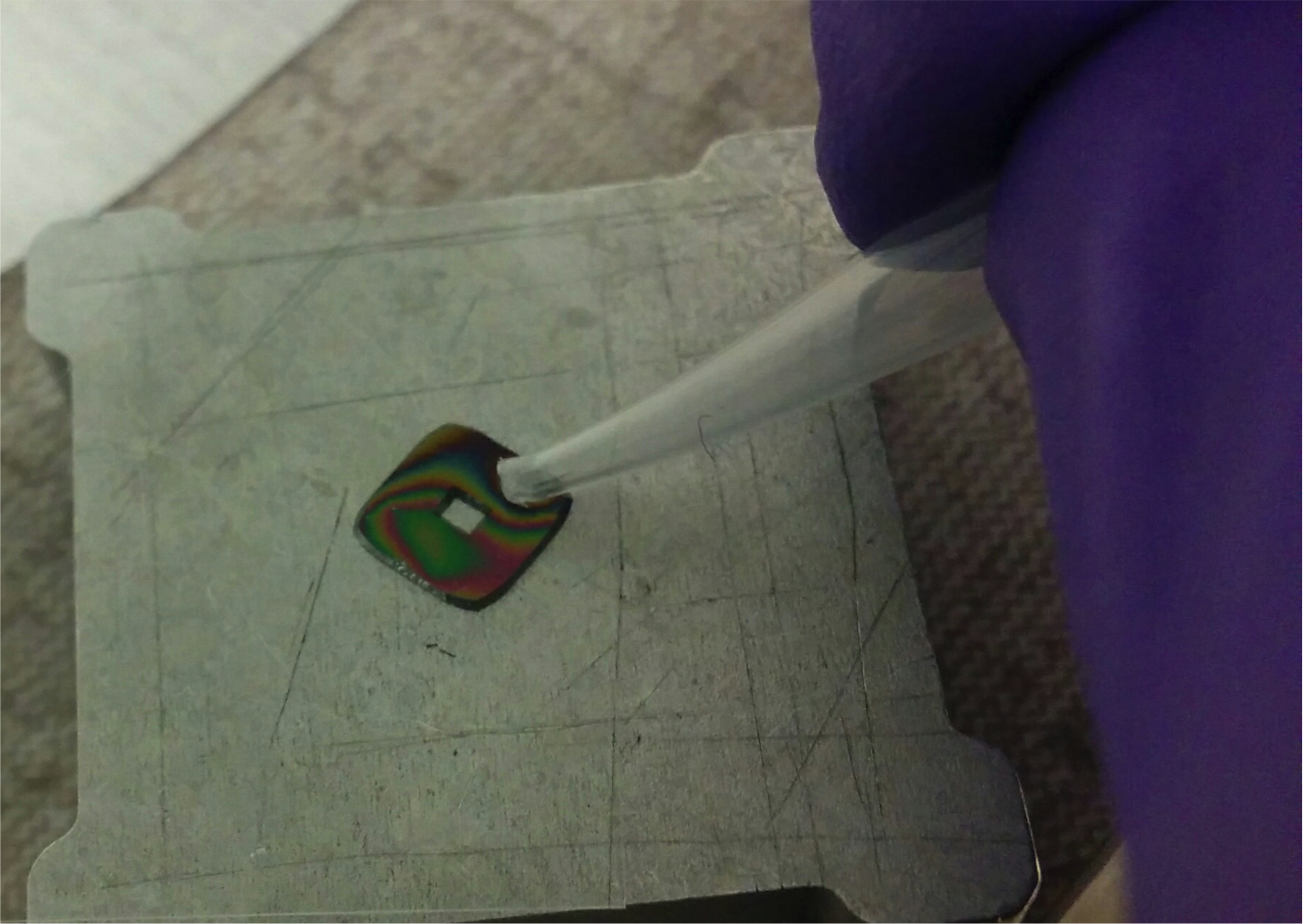
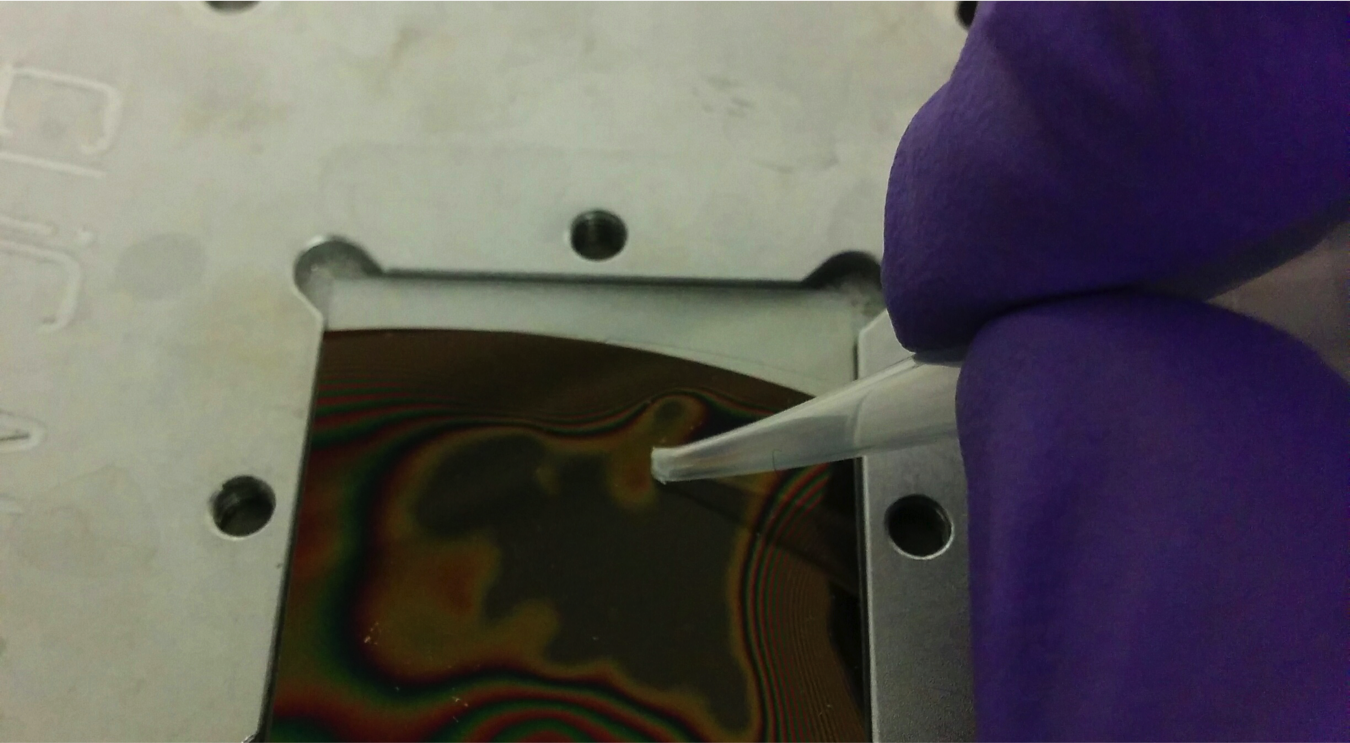
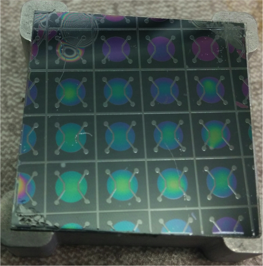
With the first failures of the device, they tried a number of different methods to improve/understand our contact problems.
- Placing chips under positive tension using a burst pressure clamp
- Improved contact, but not sufficient when released and partially melted into each other
- Characterizing the surface roughness
- AFM scans show sub-1 nm RMS surface roughnesses on the front and back of the NPN
- Characterizing the surface planarity
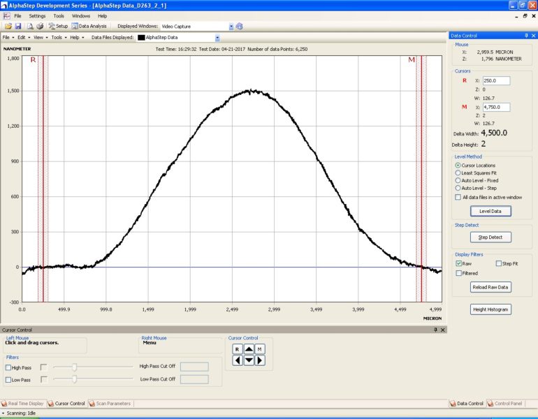
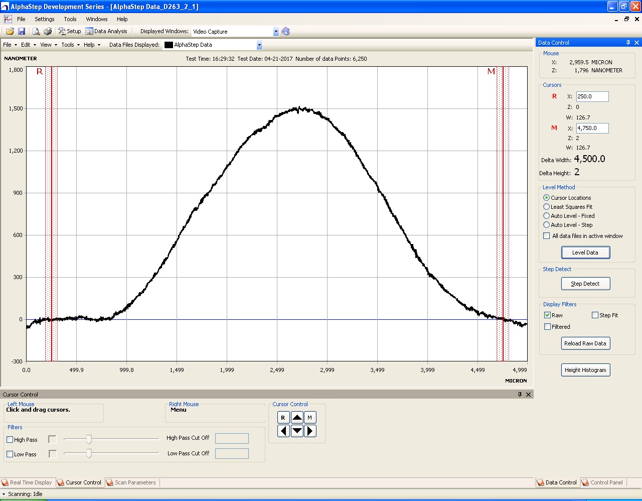
Coverglass profilometer 5mm scan. Peak deviation is well above 2 microns 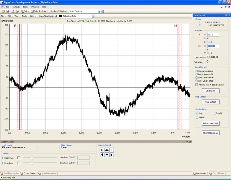
NPN profilometer 5mm scan. Peak deviation is about 300 nm, which should be tolerable in a bonding setup. - Plasma bonding both surfaces together (45 W, 2 minutes)
-
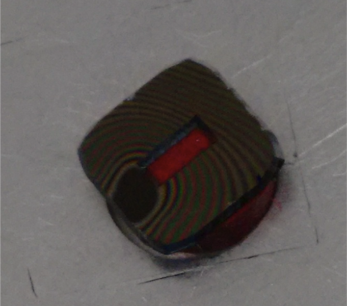
After Plasma clean, some areas can come into full contact, but Interference fringes show that it is not perfect around most of the chip.
-
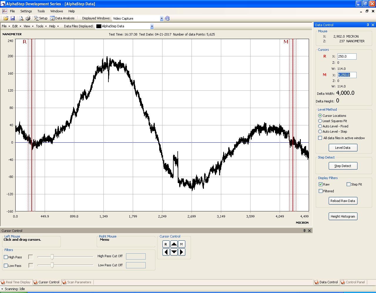
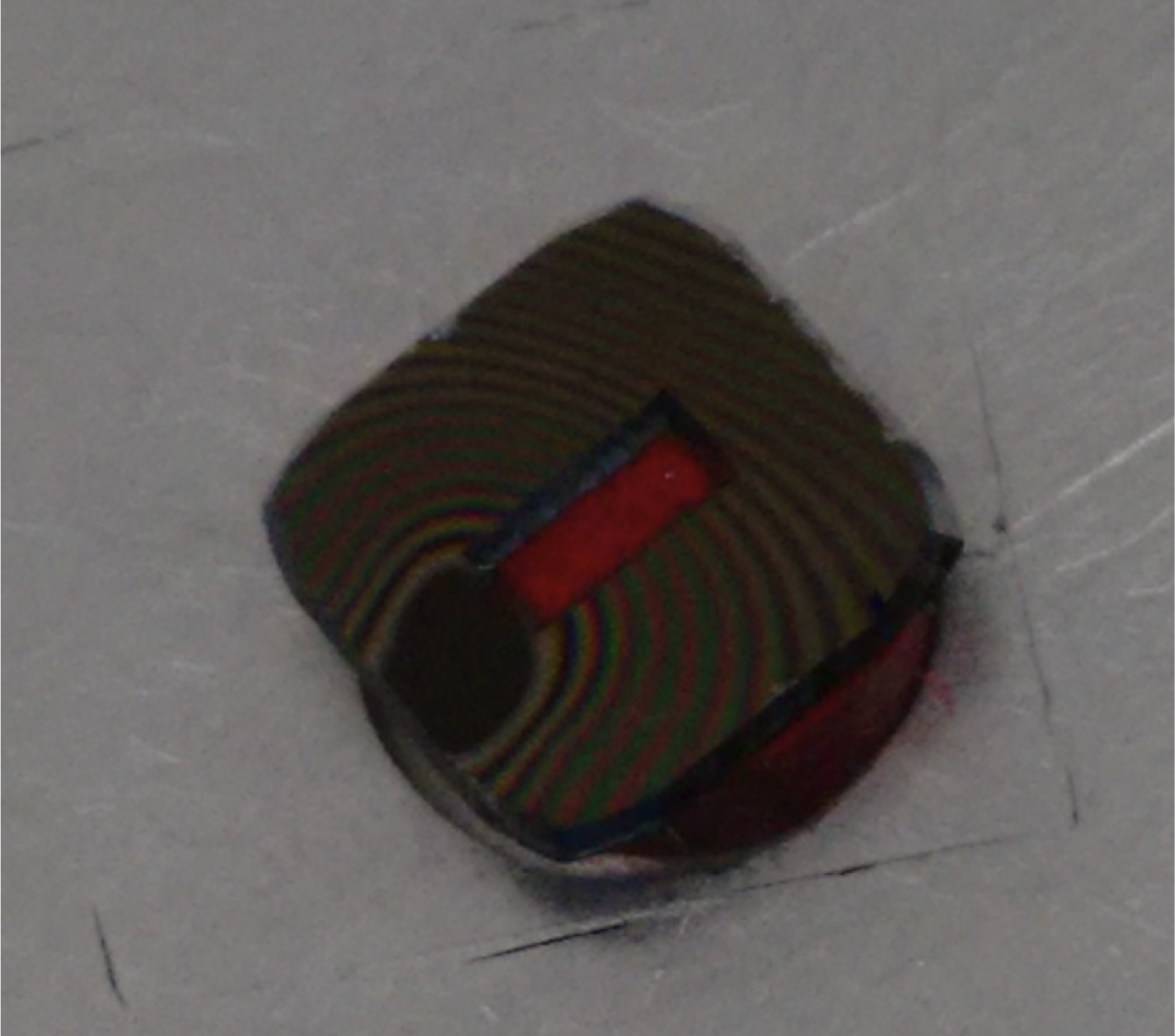
We still have some work ahead of us. Can we find a good way to planarize the glass? (planarizing the chip by polishing would most likely destroy the freestanding membrane).