Cleanroom Pore Development for Rapid Membrane Prototyping
Introduction/Motivation
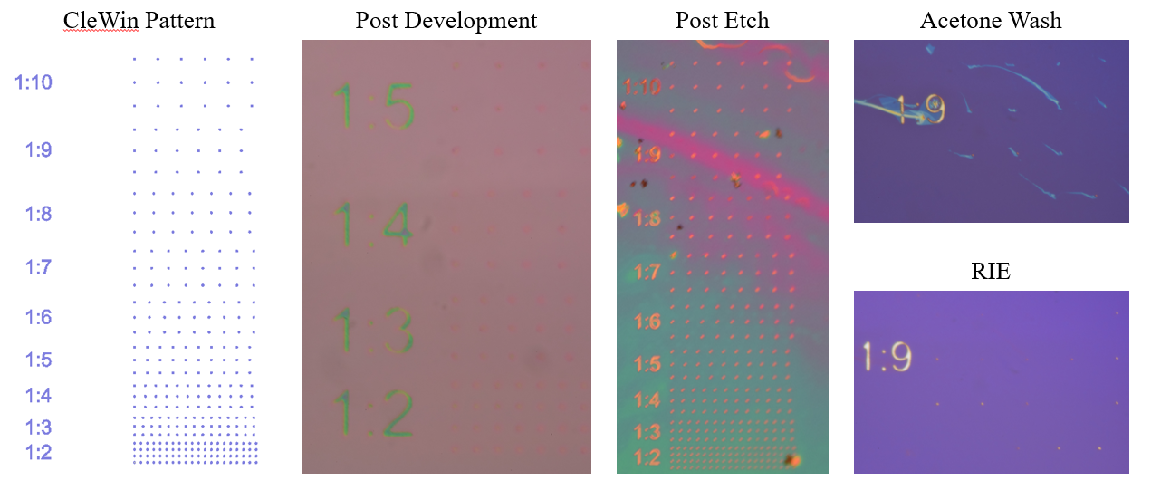
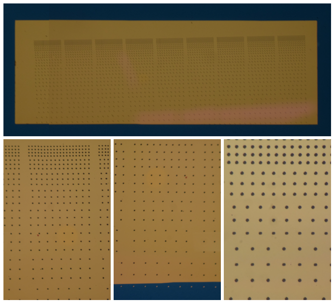
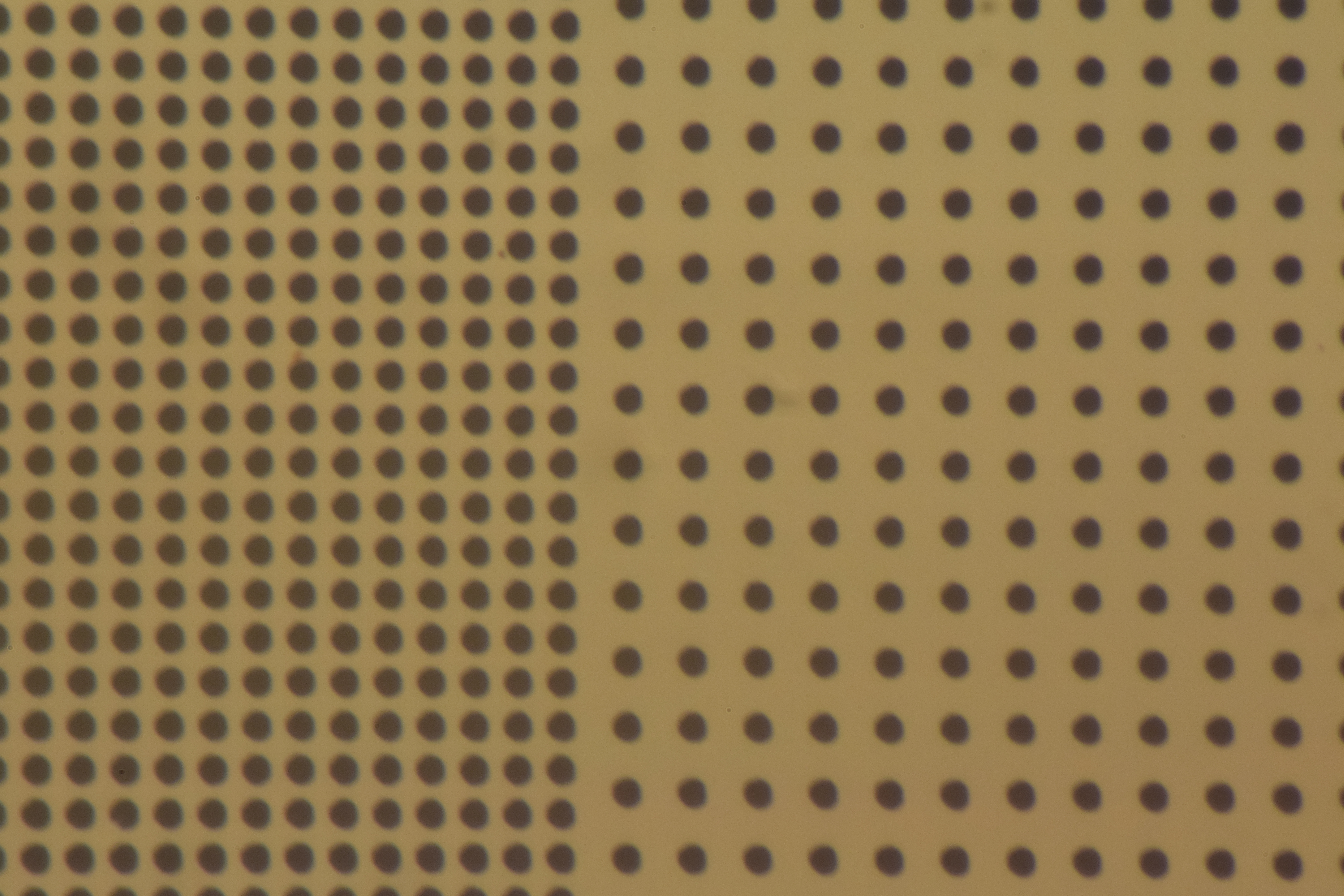
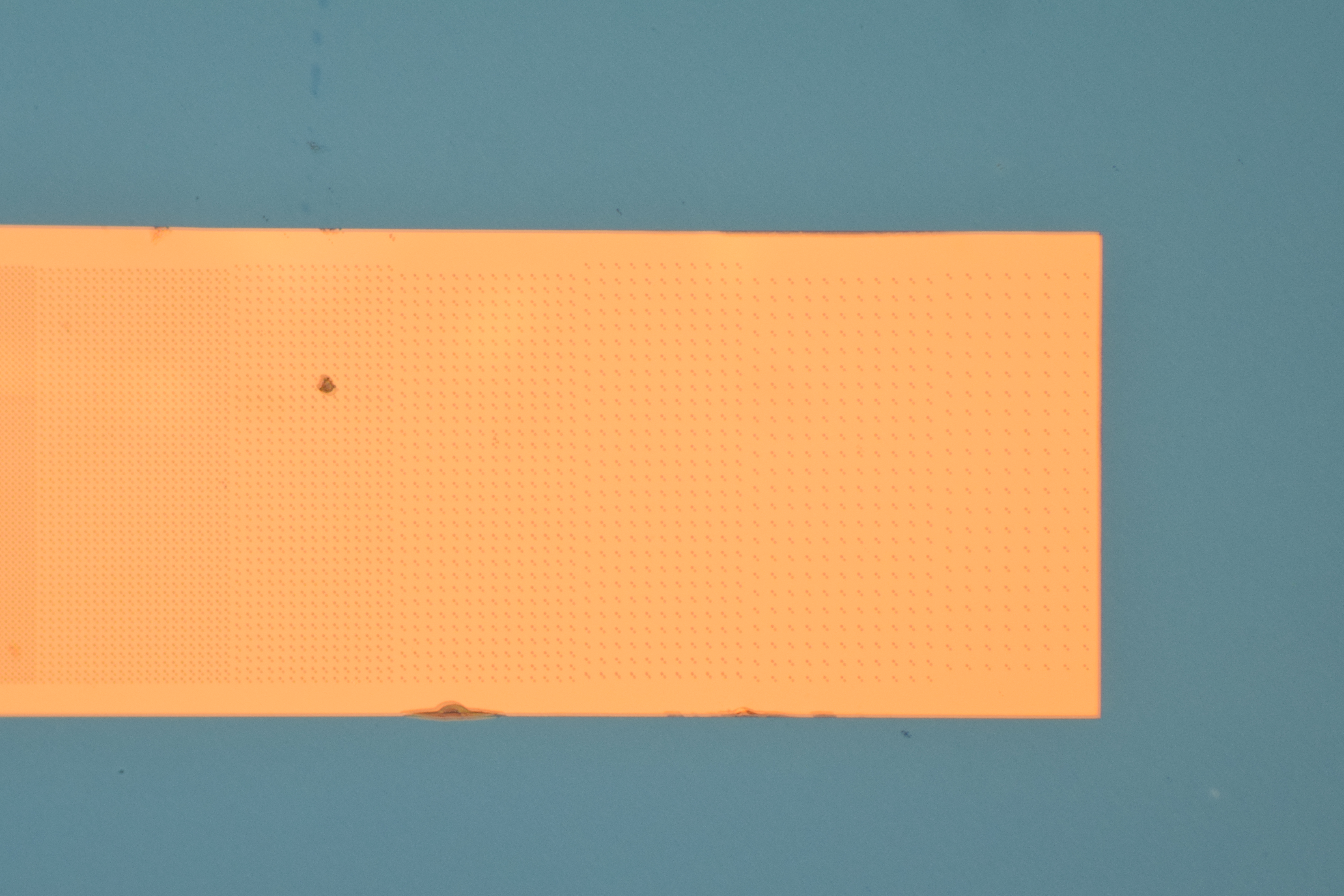
A problem many of us face in day to day research is the ability to change membrane format in a days to weeks notice. The cost of developing an entire new wafer of membranes for preliminary experiments is costly and time consuming. This cost and time increases when complex formatting is desired. All of these issues are the reason we decided to attempt to write out own membranes on site (UR Nano). The overall goal of this project was to develop a protocol for entering the cleanroom and exiting with a membrane ready for culture. The membrane format I desired was a gradient of 3 um pore spacings over a 2 x 0.7 mm membrane. The ultimate use is cell culture and high throughput adhesion experiments. If we can culture, shear, and image cells on varying pore densities all in one device, I can greatly decrease my overall experiment times.
Methods
Lithography
We start by spinning P20 HMDS in PMA and positive photoresist 1805 onto a standard NPN membrane using the following program: 1) 1000 RPM for 5 sec; 2) 7000 RPM for 50 sec; 3) 1000 RPM for 5 sec. This process takes practice, but a little unevenness in the coating is okay. Chips can be adhered to the spinner using double sided carbon tape. Soft bake the chip at 115 C for 50 sec.
Laserwriter
Using a pattern developed in Clewin 5, I exposed the photoresist to 233 mJ/cm^2. The whole process is more involved, but for reference I used the following settings: Lens 4, 30% filter, plane auto focus. Develop the pattern for 50 sec, no post exposure soft bake is required.
Etch
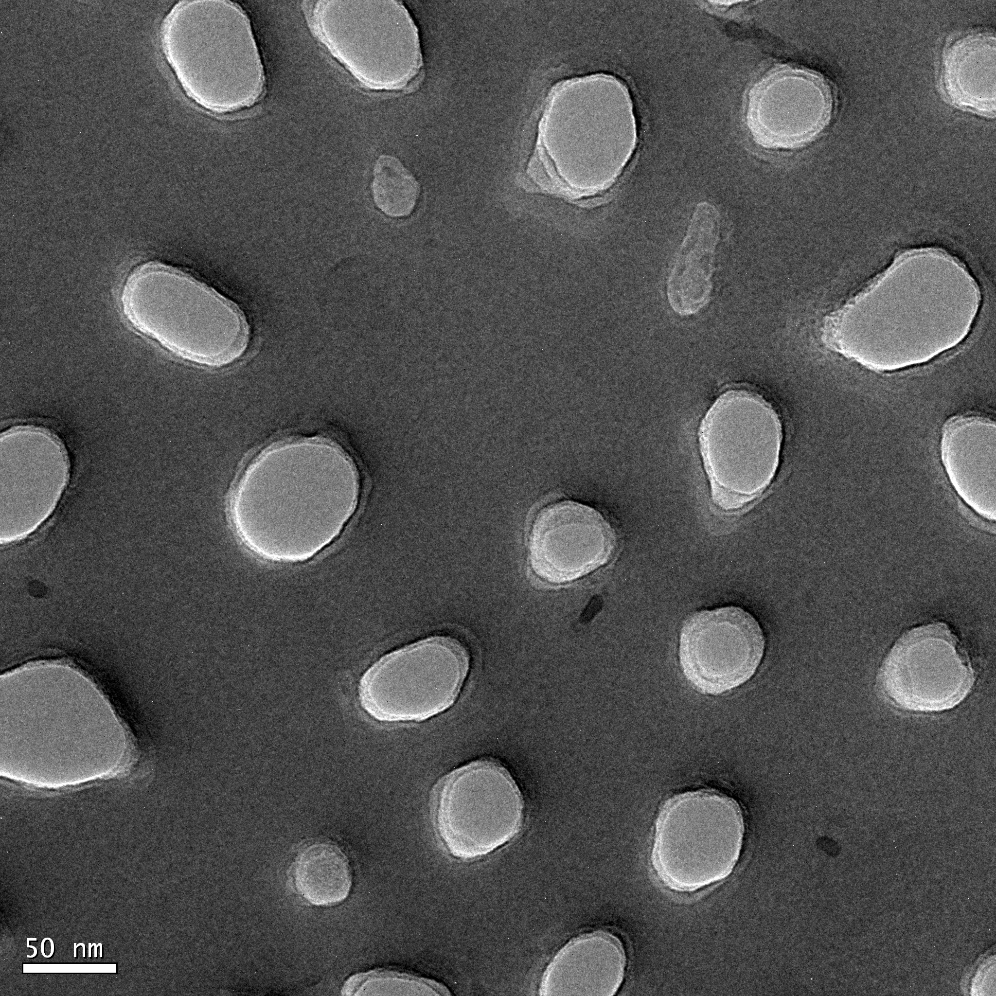
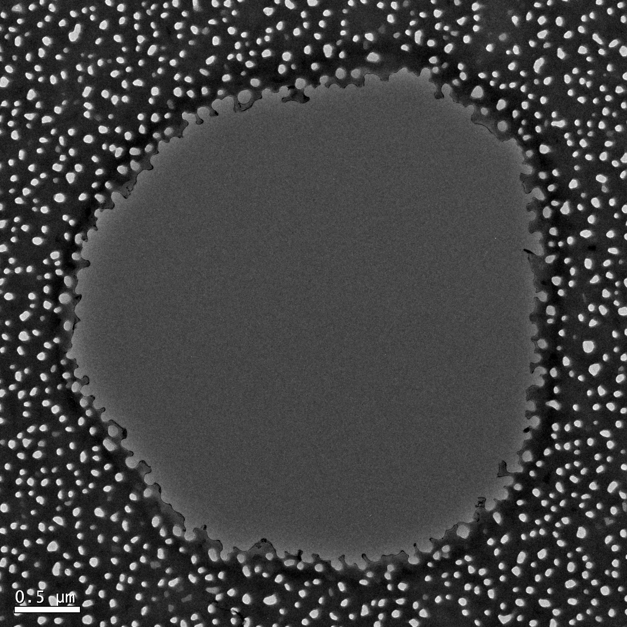
Open the O2, Argon, SF6, and CHF3 gas lines/tanks. Set the gas flow rates to the following specifications: O2 = 15 SCCM, CHF3 = 10 SCCM, SF6 = 30 SCCM. The reading pressure after opening the flow into the RIE should stabilize between 30 and 50 mTorr. Season the chamber for 5 mins (run power = 100 watts; minimize reflective power to achieve 100 watts total forward and reflective). Be sure to maintain a stable pressure and power. Once completed, the sample can be loaded. Turn off gases and pump, and vent. Place membrane on a piece of bulk silicon and pump down chamber to 5E-5. Turn gases back on and let the pressure stabilize. Run the RIE at 100 watts again for 2 mins. When completed, we can switch over to ash settings. Turn off CHF3 and SF6 and set O2 flow to 55 SCCM. The reading pressure should now be around 200 mTorr. Run the RIE at 100 watts (same calibration process; minimize reflective power) for 13 to 15 mins. Turn off gases and pump, and vent. The membrane is now clean and ready for use.
Results


Conclusion
The methods are still in early stages, but the potential for rapid membrane prototyping with real integration ability is definitely a possibility. I tried coating other materials, but found this 100 nm NPN worked best. With a little work I am sure someone could develop a process for coating those materials as well. The ability to take an old membrane and write over it could open the door to some interesting projects. As it stands, I will attempt to write some working patterns (Figure 9) and culture cells on them. I left some details out on machine use and spin coating technique, so if anyone is interested in learning this process step by step I can take you in the cleanroom and perform a quick run through. The whole process from gown up to gown down takes about 2 hours (for ~5 membranes).


Acknowledgements
Thank you to JK and Jim Mitchell for helping me get started with the lithography. Big thank you to Greg for helping me with the RIE and TEM.