Pore Density vs. Pore Radius Graphs, 15nm width and 1000RTP
The purpose of this post is to see if there is a pattern in the Pore Density vs. Pore Radius graphs at certain manufacturing conditions. The following wafers all have widths of 15nm and RTPs of 1000. The porosities range from 6.48% to 8.33%.
**** note: the y-axis label should actually read “pore density (#/nm2)” ****
SC 023:
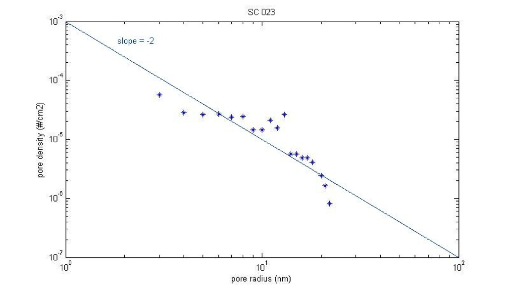
Average Pore Size: 16.0 nm
Porosity: 8.06%
Cut-Off Pore Size: 44.98 nm
Mean Roundness: 0.70, standard deviation: 0.15
Thickness: 15 nm
RTP: 1000
Ramp Rate: 10 C/s
SC 025:

Average Pore Size: 18.7 nm
Porosity: 7.37%
Cut-Off Pore Size: 47.70 nm
Mean Roundness: 0.74, standard deviation: 0.15
Thickness: 15 nm
RTP: 1000
Ramp Rate: 10 C/s
SC 066:

Average Pore Size: 21.8 nm
Porosity: 7.06%
Cut-Off Pore Size: 32.89 nm
Mean Roundness: 0.82, standard deviation: 0.11
Thickness: 15 nm
RTP: 1000
Ramp Rate: 100 C/s
SC 077:
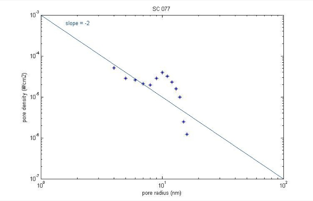
Average Pore Size: 16.6 nm
Porosity: 7.37%
Cut-Off Pore Size: 32.67 nm
Mean Roundness: 0.79, standard deviation: 0.13
Thickness: 15 nm
RTP: 1000
Ramp Rate: 100 C/s
SC 078:

Average Pore Size: 15.5 nm
Porosity: 6.48%
Cut-Off Pore Size: 27.67 nm
Mean Roundness: 0.79, standard deviation: 0.15
Thickness: 15 nm
RTP: 1000
Ramp Rate: 100 C/s
SC 130:

Average Pore Size: 17.5 nm
Porosity: 8.04%
Cut-Off Pore Size: 30.05 nm
Mean Roundness: 0.83, standard deviation: 0.11
Thickness: 15 nm
RTP: 1000
Ramp Rate: 100 C/s
SC 131:
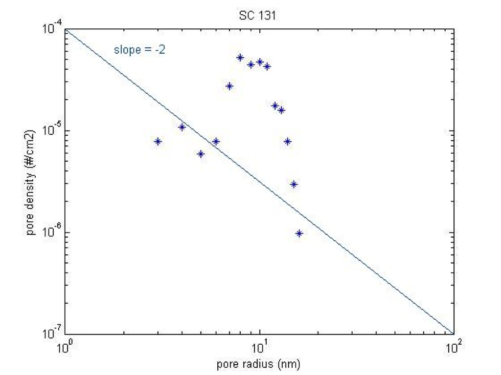
Average Pore Size: 18.5 nm
Porosity: 8.33%
Cut-Off Pore Size: 31.44 nm
Mean Roundness: 0.82, standard deviation: 0.11
Thickness: 15 nm
RTP: 1000
Ramp Rate: 100 C/s
SC 132:
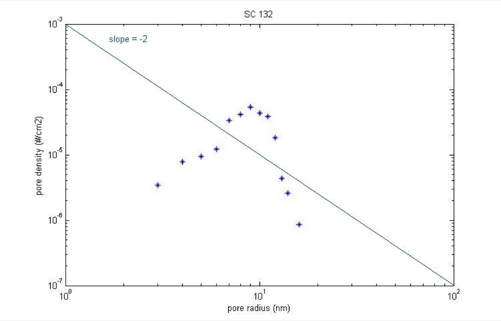
Average Pore Size: 17.8 nm
Porosity: 7.12%
Cut-Off Pore Size: 31.96 nm
Mean Roundness: 0.82, standard deviation: 0.11
Thickness: 15 nm
RTP: 1000
Ramp Rate: 100 C/s
SC 141:
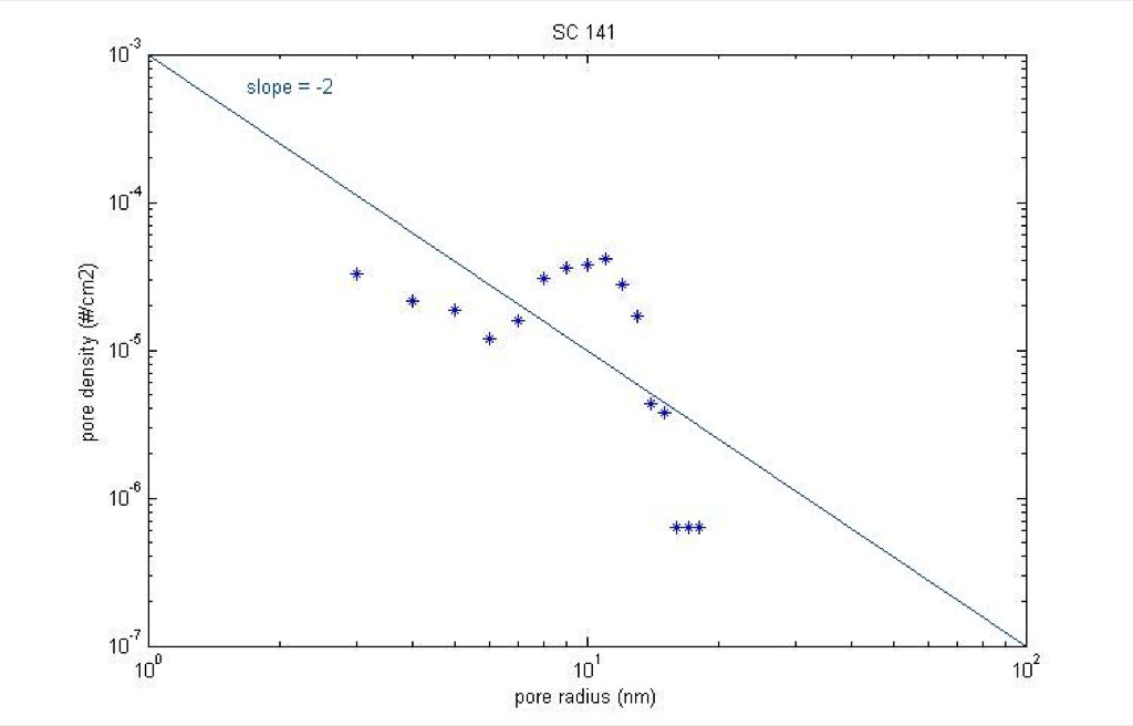
Average Pore Size: 17.1 nm
Porosity: 7.90%
Cut-Off Pore Size: 36.99 nm
Mean Roundness: 0.82, standard deviation: 0.12
Thickness: 15 nm
RTP: 1000
Ramp Rate: 100 C/s
SC 225:

Average Pore Size: 14.9 nm
Porosity: 6.86%
Cut-Off Pore Size: 33.29 nm
Mean Roundness: 0.77, standard deviation: 0.14
Thickness: 15 nm
RTP: 1000
Ramp Rate: 100 C/s
Conclusions:
Interestingly, the wafers with ramp rates of 100 C/s show clear peaks at a pore radius of 10nm while the wafers with ramp rates of 10 C/s do not exhibit clear peaks.
interesting… Several thoughts. First, I would say there is a small peak in the 10 C/s samples simply it is much less pronounced. Second, the roundness of the 10C/s samples is lower. Third, if say the annealing temp is changed or some other parameter is changed, does a peak still exist and if it does, is its location the same?