A new idea to fabricate nano pocket membrane
Starting in July of 2021, we began a new idea fabricating the nano pocket membrane to capture and release the EVs. From then until now we have successfully fabricated nano pocket membranes by using a lithography method. We faced challenges in parylene etching and resolve it by using two etching machines, i.e. Trion Phantom III RIE and the plasma cleaner. This post shows the methodology of creating the nano pocket membranes and the preliminary results.
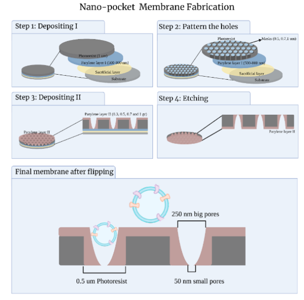
Figure 1: Fabrication process overview.
Membrane Fabrication :
Figure 1 provides an overview of the fabrication process. The fabrication process is divided into 4 steps: depositing I, porous pattern, depositing II, and etching. The first process is creating the layers by depositing them over the Si wafer. We started by depositing a Sacrificial Layer (SL) to peel off the membrane in the further steps. Then a Parylene layer (PAR), named Parylene I in the figure, is deposited to protect the SL layer from the next layer which is the Photoresist (PR) layer. Finally, a layer of 1 um PR is deposited over PAR layer I. To validate the parylene deposition, a NanoSpec Spectrophotometer is used to measure the PAR thickness.
The goal of the second step is to create pores in the PR layer by using Advanced Semiconductor Materials Lithography (ASML). Different masks are used (0.5, 0.7, and 1 um) with usually 8% porosity. Figure 2, shows the pores on the PR layer. We observe that the pores sizes are around 500 nm and all have sharp edges.

Figure 2: Pores in the PR layer by using ASML.
The main process in the third step is creating the nano pocket porous by depositing PAR on top of the PR layer using a parylene coater. Different amounts of PAR are applied (0.1, 0.3, 0.5, 0.7, 1 and 1.2 gr) depending on the PAR porous size (we mostly used 0.5, 0.7, 1 and 1.5 um). To validate the second parylene deposition, a witness sample was placed near to the wafer then we used a NanoSpec Spectrophotometer to measure the PAR thickness. Figure 3, shows a 100 nm PAR deposition on top of the 700 nm PR. The porous sizes were reduced to around 500 nm. Also, porous edges are soft unlike before the deposition. Increasing the PAR deposition to 0.5 gr, around 500 nm reduces the pore size to the range of (120 – 150 nm) as illustrated in Figure 4.

Figure 3: A 0.1 gr PAR deposition on top of PR

Figure 4: A 0.7 um porous with 0.5 gr PAR deposition.
The expected output of this last step is to have the final nano pocket membrane. We etch the PAR layer I to form the small pores. The etching time varies based on PAR layer I. The etching machine used is Trion Phantom III RIE. The energy parameter is set to 100 w. Other parameters are set as the following: O2 = 40 sccm while Sulphur hexafluoride (SF6) = 0 sccm. Figures 5, 6 show the small porous on the same membrane with different etching times. The etching time difference between the two figures is trivial. Yet, the porous size difference is huge. There are no pores at all with 20 sec time. We faced this inconsistency with all etching experiments using the RIE machine. We could not find any relation between results and etching time which prevent us from controlling the results. Figure 7 is one of the best pocket shapes we obtained. However, we could not reproduce it (even though we tried 12 times) using the same parameters and membrane due to the inconsistency problem.

Figure 5: Pores with 25 sec etching time.
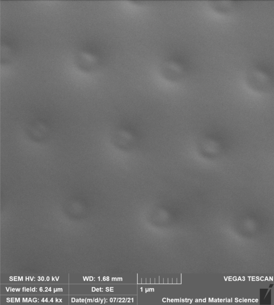
Figure 6: No pores with 20 sec etching time.
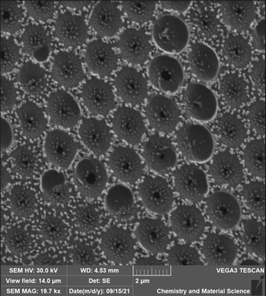
Figure 7: A pores size 1.5 um and the small pores are around 200 nm (the parylene amount is 0.5 gr)
After constantly facing the inconsistency issue during etching, we consider replacing the RIE machine with the plasma cleaner machine. The plasma cleaner machine’s maximum energy is 30 w with adjustable O2 flow.
First, we checked the etching rate for the plasma cleanere by etching a known parylene sample for 20 min then calculating the etching rate. We found the best time to be 5 nm/min. For a 1300 nm parylene I, we need around 4:30 hours to etch it. We tried to do 3 to 7 hours for 5 samples. By using the plasma cleaner machine, we were able to control the etching to have different porous sizes based on etching time because the relation is linear as we found.

Figure 8: Nano-pocket membrane with top porous is 500 nm and the bottom around 250 nm using plasma cleaner machine for 5:30 hours.
Future work:
- Confirming the etching time and the pores size linear relationship on the plasma cleaner
- Checking the membrane’s ability to capture and release the beads.