The objective of last week’s production was to track down the source of Cu contamination. The good news is that none of the wafers showed signs of Cu. The bad news is we are not sure why it has disappeared all of the sudden. Chris and I observed that there are particles in the well of the membranes composed of Si and Pt, but these do not seem to affect the membranes like the Cu particles did.
Process parameters
Wafers 302, 303
- initial SC1 (organic) & SC2 (metal) clean
- no scrub clean
- no SC1 clean prior to deposition (typically done)
- room temperature deposition
- 950 C RTP for 120 s
Wafer 304
- initial SC1 (organic) & SC2 (metal) clean
- scrub clean
- no SC1 clean prior to deposition (typically done)
- room temperature deposition
- 1000 C Ar FA
Wafer 307
- initial SC1 (organic) & SC2 (metal) clean
- scrub clean
- no SC1 clean prior to deposition (typically done)
- room temperature deposition
- 950 C RTP for 120 s
The return of “round” pinholes
All of the wafers showed signs of pinhole defects in moderate density, with the exception of wafer 302. It seems that there is wafer-to-wafer inconsistency with respect to the cleanliness, since wafer 302 and 303 were attempted mimics of each other. These pinholes appear to be a result of a failure in the oxide mask caused by contamination prior to deposition. Note that a SC1 clean was not performed before deposition due to technical difficulties at RIT. The scrub-clean vs. no-scrub wafers did not show a significant difference with respect to pinhole density (both had pinholes present).

Optical image from wafer 304 (-1,4)
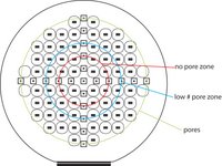
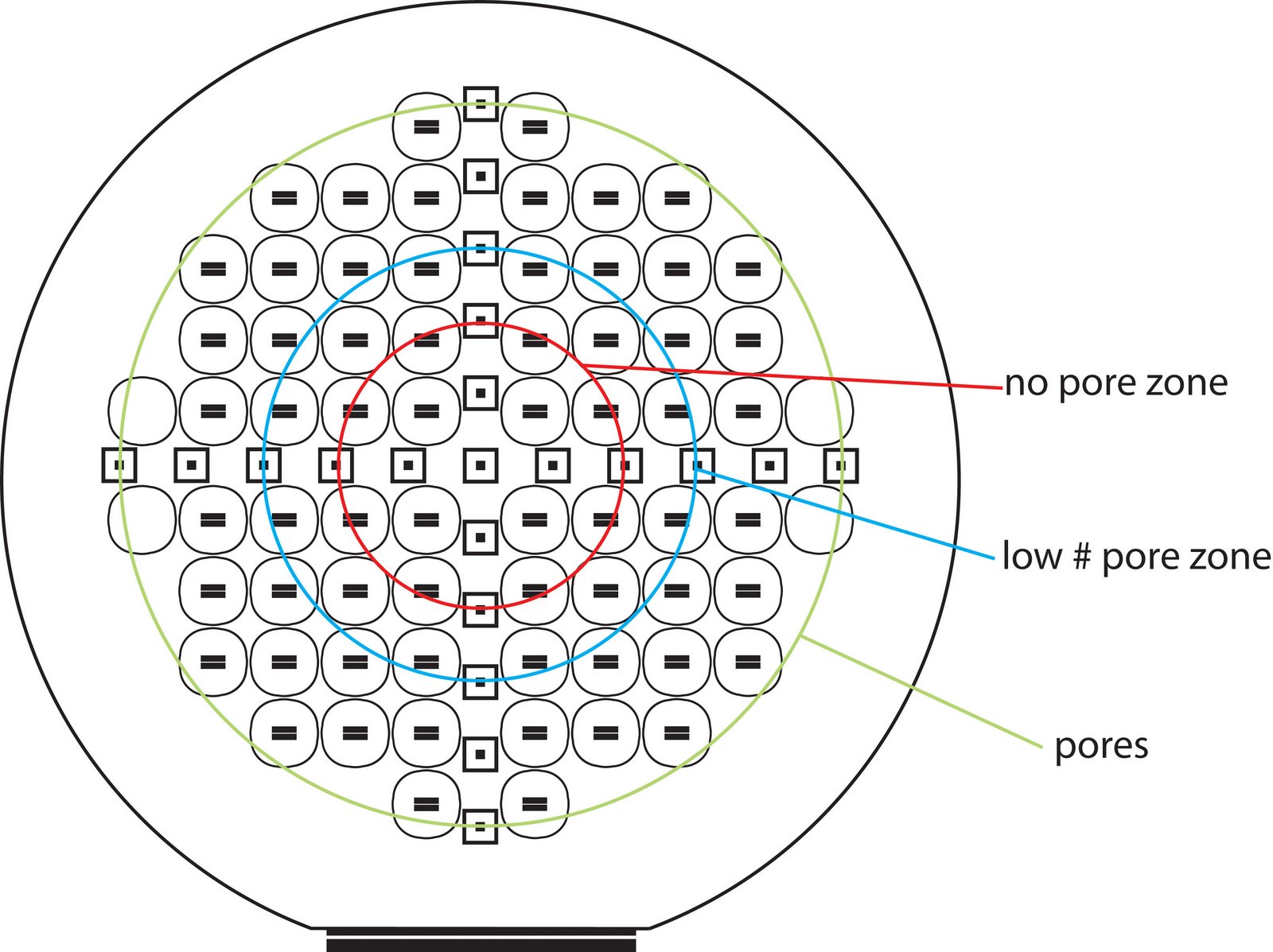
Pore non-uniformity across wafer
This non-uniformity is not a new occurrence. However, this set shows no through-pores in the center membrane samples. As you move towards the edge samples, more pores start popping through. Below is a chart defining the different “pore zones”.
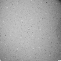
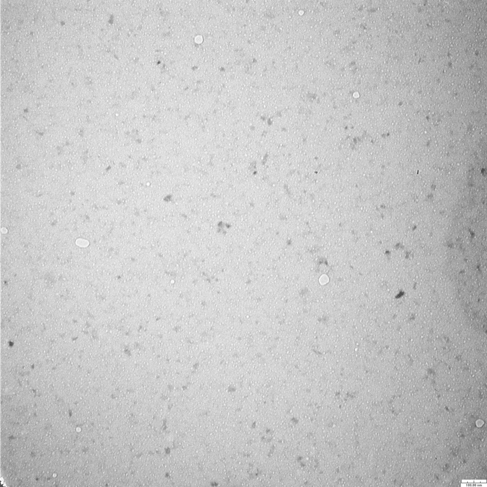
 The corresponding TEM images from each zone are shown here:
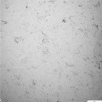
wafer 302 (0,0)

wafer 302 (3,0)
 wafer 302 (4,0)
 wafer 303 (4,0)
As you can see, there is an increase in the number of pores in samples closer to the edge of the wafer. The 302 (0,0) sample shows texture which indicates pore formation is starting, but has not fully developed. I was not able to focus on these features, which leads me to believe that the structures do not fully penetrate the film. Interestingly, the pore sizes seem to be consistent; it is only density that varies.
Wafers that were placed in the RTP only and furnace anneal only showed this variability. This is significant, since the rate of heating is much faster in the RTP vs. FA.
The most likely culprit is the deposition tool. Because the throw distance of our target to substrate is small and the RF plasma plume is shaped like a “doughnut”, there is a variable path length over which the Si atoms are deposited on the 4″ wafer. The new sputter system should remedy this with the option for multi-angle deposition and an increased throw distance. The non-uniformity has been verified via ellipsometry. It’s unclear why the thicker film near the edge of the wafer has a higher density of pores.
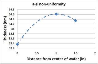
Although the non-uniformity is within %5, this is apparently large enough to cause a change in the pore morphology.
The one piece of good news is that wafers 302 and 303 showed similar morphology, which is expected since they were processed identically.
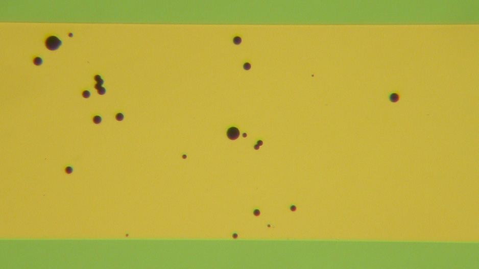 Optical image from wafer 304 (-1,4)
 The corresponding TEM images from each zone are shown here:
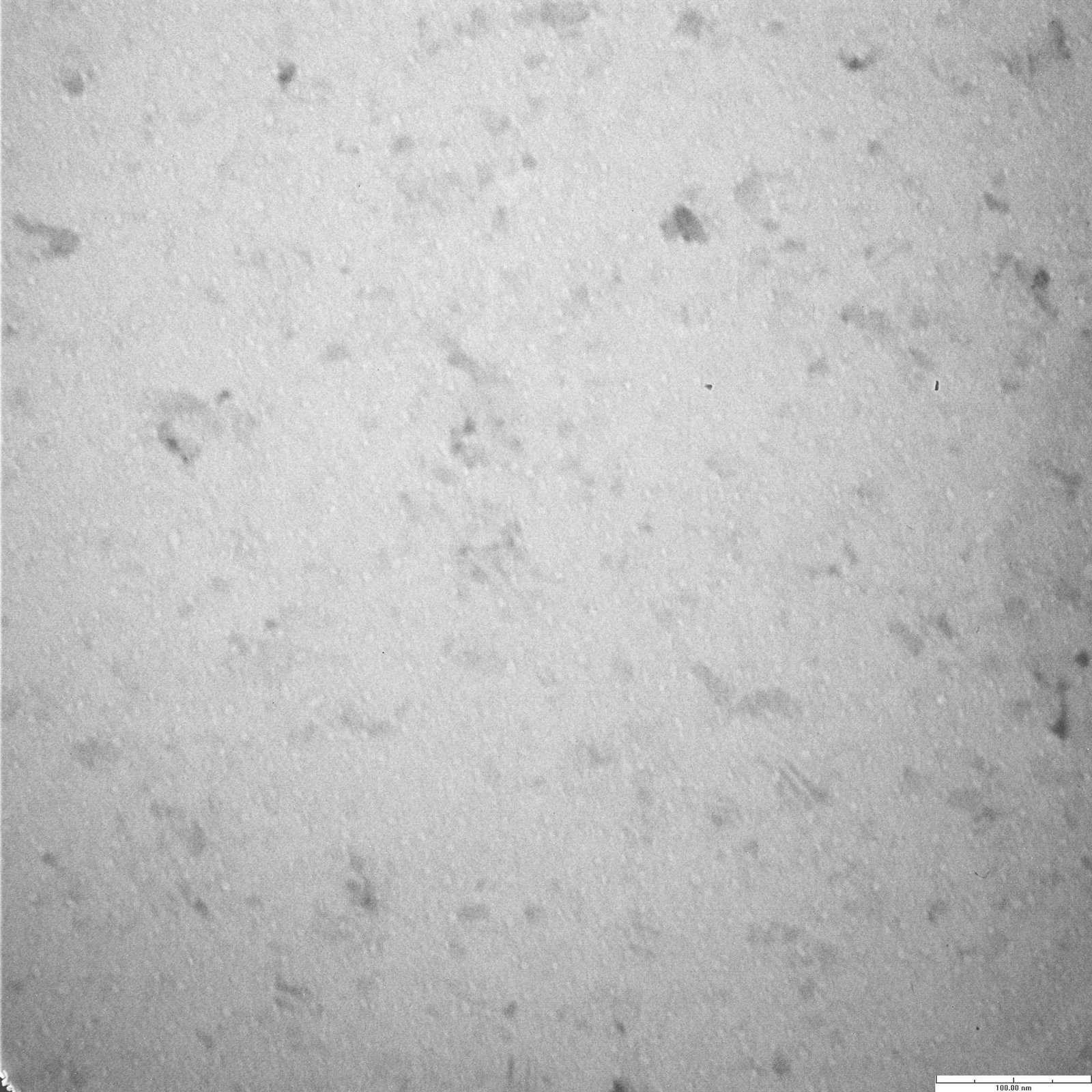 wafer 302 (0,0)
 wafer 302 (3,0)
 wafer 302 (4,0)
 wafer 303 (4,0)
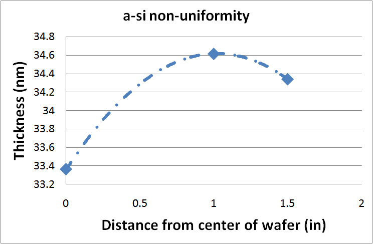