W509X Burst Pressure and Air Permeability
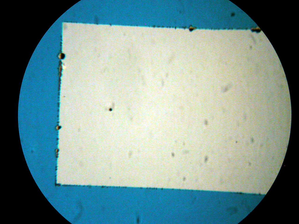
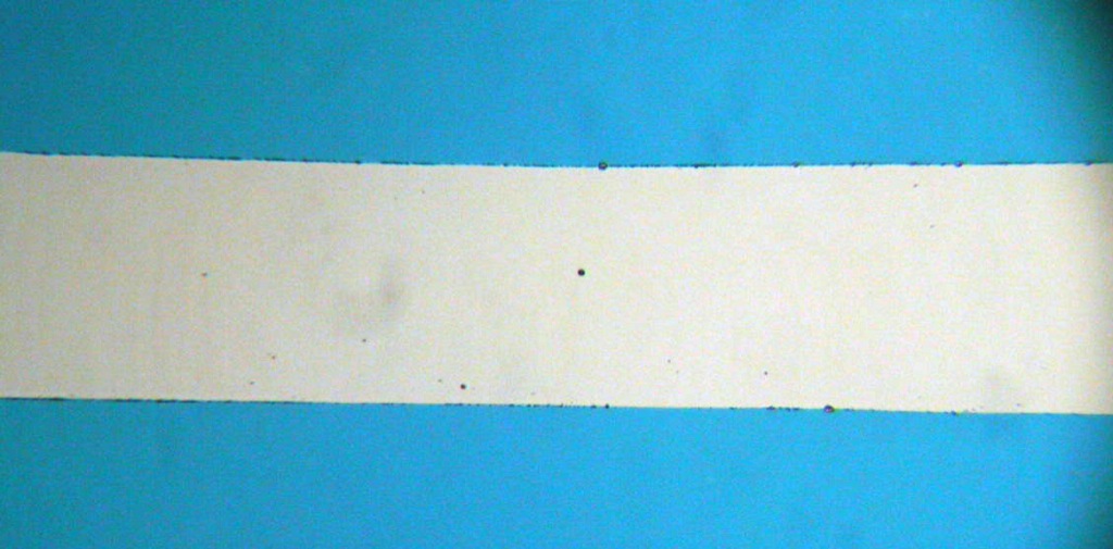
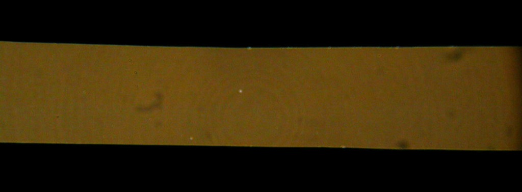
W509X, with single 100um by 1000um slits, was tested for air permeability and burst pressure. Prior to testing, I inspected all membranes for pinholes.; every sample had pinholes on the membrane perimeter, as shown below. The first two images are in reflection mode (pinholes appear black) and the last is a transmission image (pinholes appear white).
Interestingly, there were very few pinholes on the membranes other than on the outer perimeter. Despite the pinholes I tested some samples for air permeability and burst pressure. Of the 5 samples I removed 3 broke when the air permeability test was started, indicating these samples have burst pressures less than 1 psi. The results for the two remaining samples (1,-1) and (4,-3) are shown below.
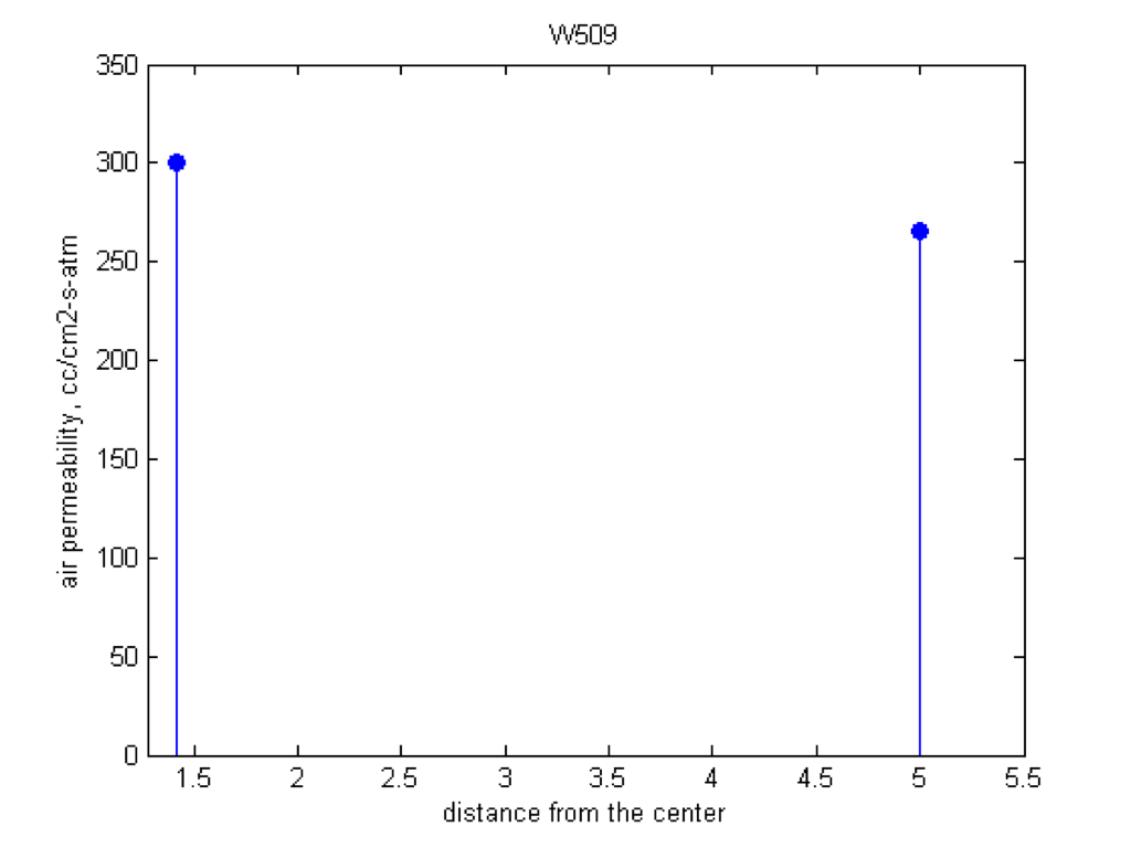
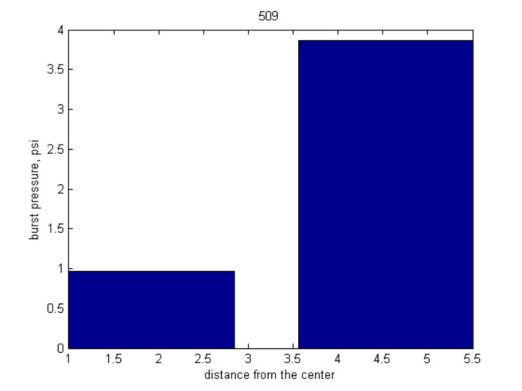
While the samples tested had pinholes they had similar air permeabilities; I am unsure if this is a coincidence or if the perimeter pinholes are not taking part in the permeability for some reason.
Why are we testing 509 now? Hasn’t this material been around for weeks? Is there a particular question we are trying to address? If so, what is the answer.
Jim,
This is actually wafer “509X”. This was a wafer from the 6-wafer experiment Dave and I conducted over this weekend/Monday. I had to label them with “X” because some of the wafers were accidentally scribed with a duplicate #.
Also from this experiment are wafers labeled:
“510X”, “511X”, “512X”, “513X” and “400”.
Sorry about the confusion. I lost track of wafer #’s for awhile. This week, we are back on track and will be starting with wafer #600.
It seems that these “tears” along the edges of the membrane are caused by stress/strain during the high temp anneal. From the same wafer (509), I looked at three samples: amorphous, RTP 950 C, RTP 1050 C. The amorphous and 950 C had almost no defects. Wafer 565 was annealed at 950 C and showed high burst pressures but no flow. The 1050 C is what Karl took pictures of in this post.
I’m currently depositing a three layer film on wafers with thinner oxide. I will also back off on the RTP ramp rate in an effort to reduce the strain in the film during annealing. I have a feeling that large/high-porosity membranes may come with the side effect of pinholes… we’ll see.