AFM – new tips and wafer characterization
I ordered some new AC160 tips last week from Asylum and got on the AFM Thursday to test them out. I think they solved some of the problems I was running into over the last few weeks. Mainly, I was finally able to image entirely in repulsive mode (which was impossible with the older tips). All of these scans were 5×5 microns.
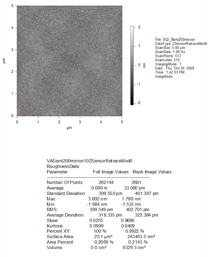
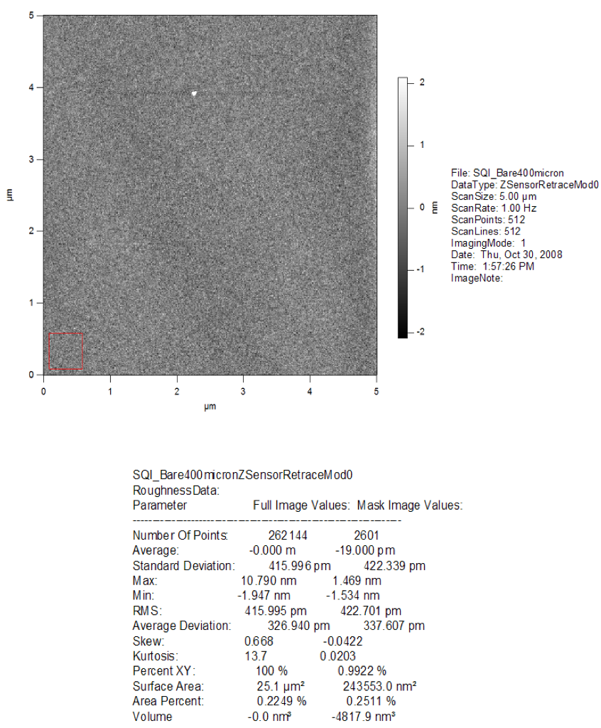
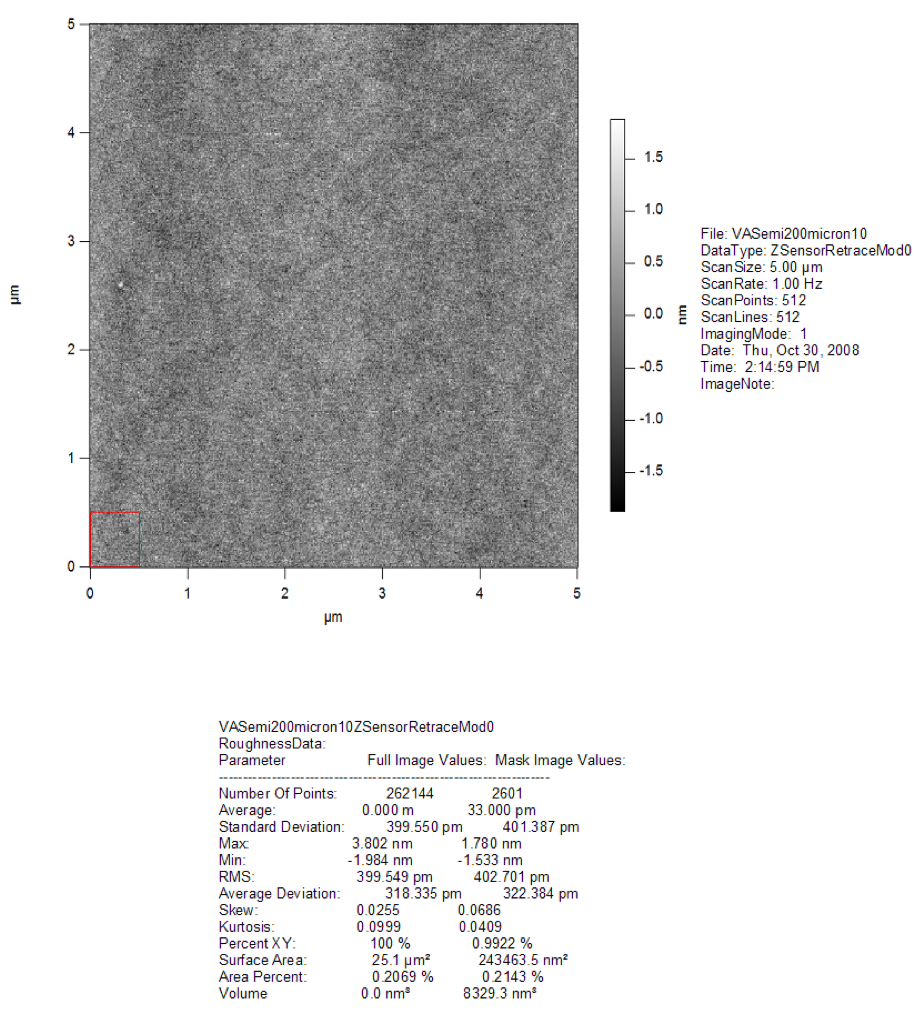
Chris gave me a bunch of wafers from SQI (200 and 400 micron bare) and Virginia Semi (1000 Angstrom oxide), so I imaged these. For each image, I selected a ROI (red box) to calculate a roughness. The roughness calculation summary is below each image. For all of the wafers, the roughness was essentially the same (~0.4 nm). It seems like the 200 micron wafer has more extremely small particles than the 400 micron wafer.
This is the 200 micron wafer from SQI:
And the 400 micron bare SQI wafer:
And the Virginia Semi wafer with 1000 Angstron oxide:
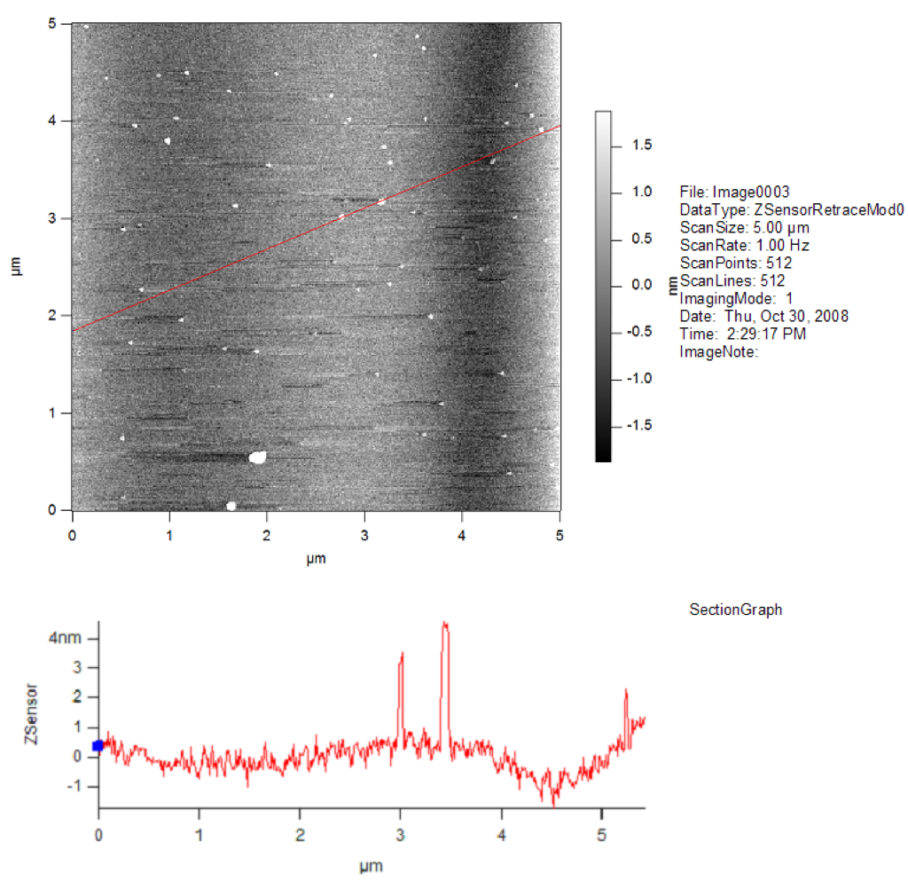
Just to confirm that the images I got from the AFM with the old tips were real, I re-scanned the Megasonics (1 run, 225W) cleaned wafer from Virginia Semi. With this image, I had problems with phase hopping when the tip hit features, but this scan confirms that this wafer is truly contaminated with particles.
Have we been able to confirm that the dirty wafers generate more pinholes? Or better yet … are the clean wafers, pinhole-free?