Process Variables to imitate wafer 1085 npMgF2/npAu
Summary
I want to imitate the material properties from 1085 as they have given us the best SERS performance to date. We have the best information that we’ve ever had before imitating the nanostructure and nanotopology from the MgF2. Our belief is that getting infilled Au close together in a nanopore dramatically enhances the electric field and dominates the SERS behavior of the nanomaterial. We can effect changes in the npAu layer by choice of substrate properties, MgF2 deposition conditions, and Au deposition conditions, as these all will have an impact on the final NPN structure.
Best SERS active material
- 1085 npMgF2 was produced end of January 2014 (etched 1/27/14)
- I was also producing npMgF2 chips from 1081 NPN at this time; these were made Feb-June 2014.
- Sent over to Nottingham in Gel boxes
- Sat around for a little while (months)
- Kevin and Cristian evaporated Au on top of the npMgF2 with 50 nm Au thickness, platen rotation using a simple Au sputterer.
npMgF2 1085 Structural Information
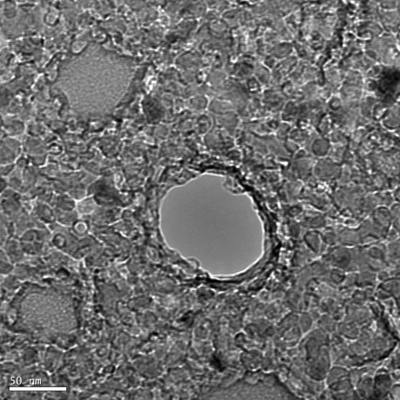

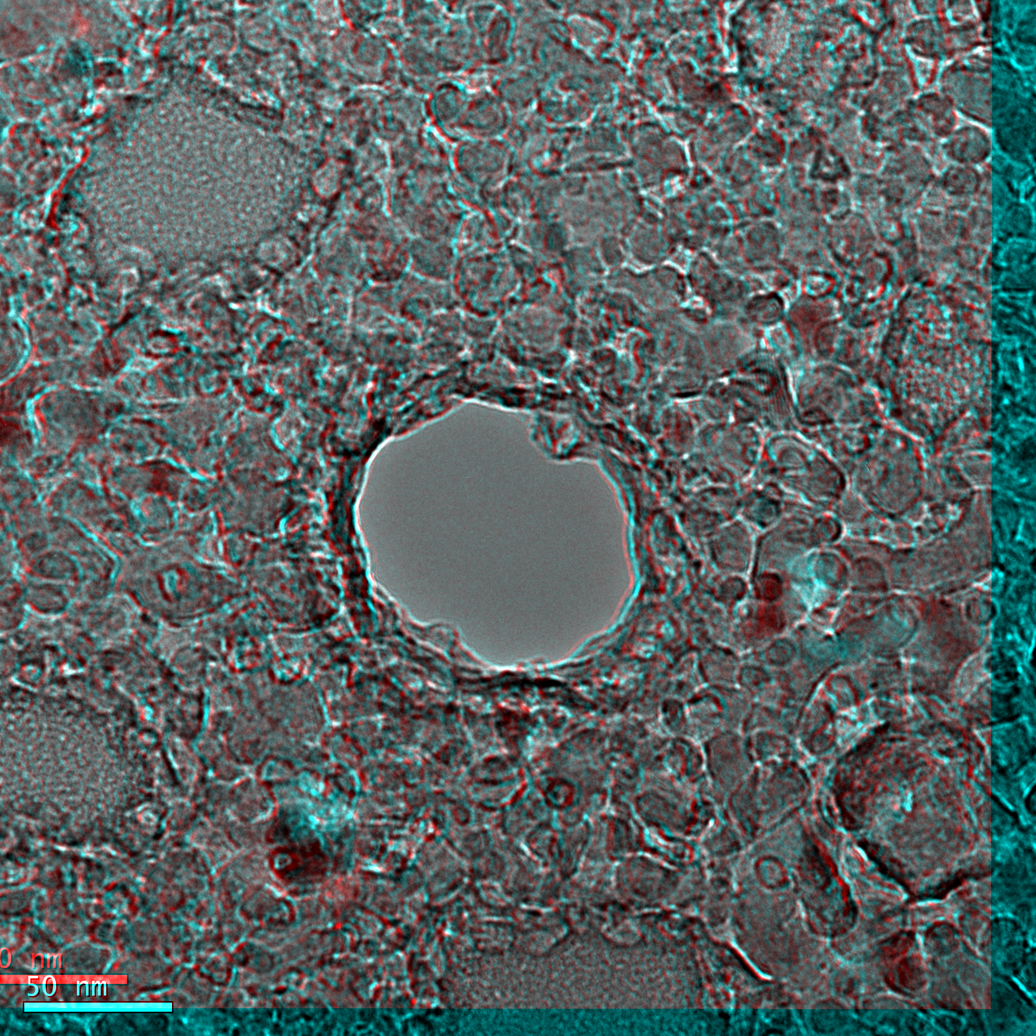
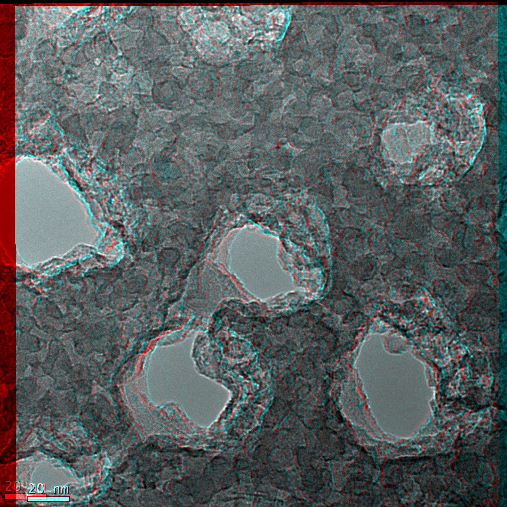
Tomogram of 1085 MgF2
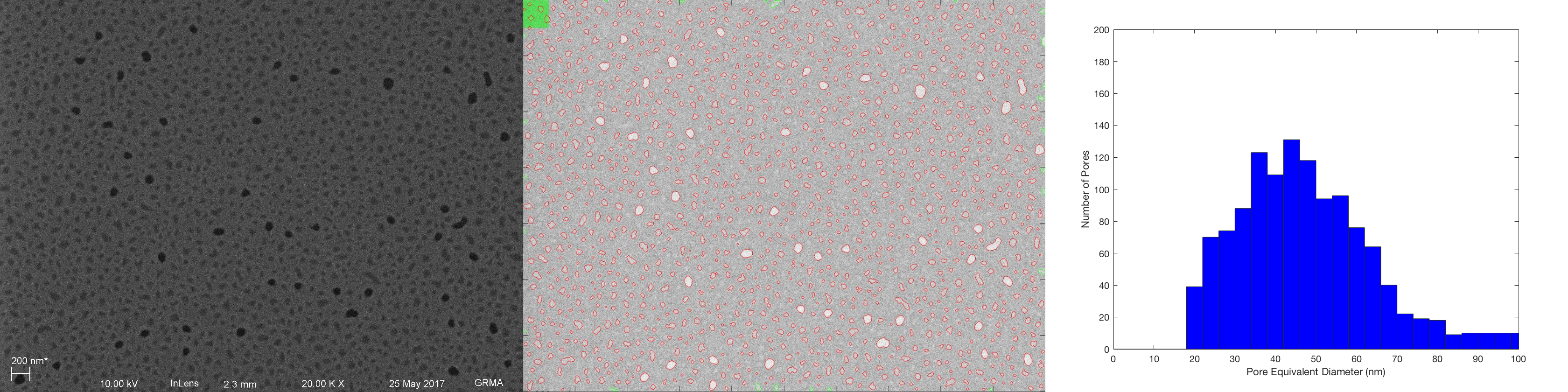
Quantifiable Parameters
- 1085 npMgF2 thickness = 50 nm
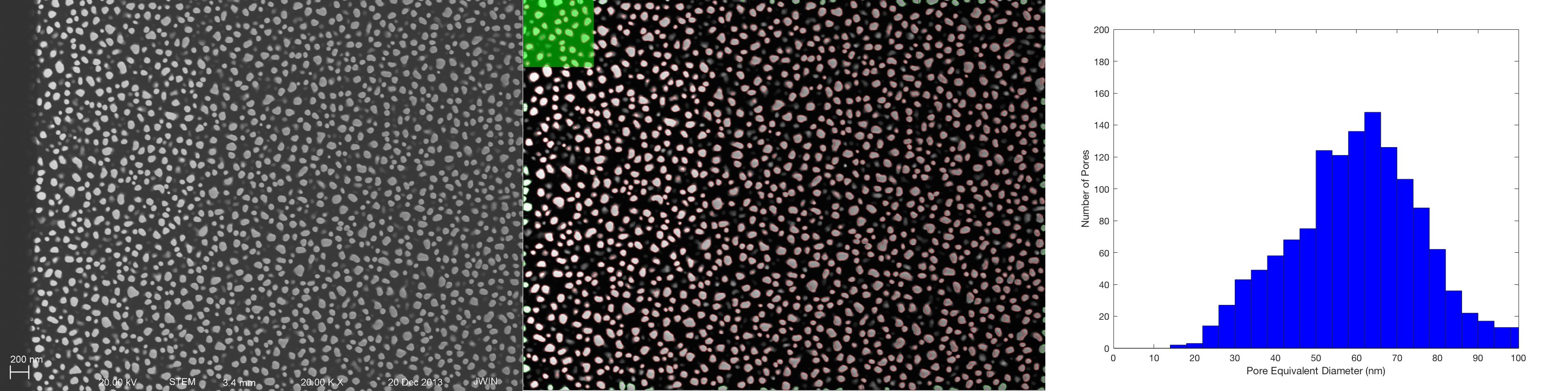
- 1085 npMgF2 pore size = 47.5 nm average, normal distribution
- 1085 npMgF2 Porosity = 11% (note this does not account for the blocked pores observed on the SEM)
- 1085 npMgF2 surface grain size = 3-5 nm (based on observations from my tomogram)
- 1085 npMgF2 bulk grain size = 10-20 nm
- 1085 NPN Pore size = 61 nm average, normal distribution
- 1085 NPN thickness = 50 nm
- 1085 NPN Porosity = 20%
The 50 nanometer thickness deposition results in infilling, narrowing pores by 10-15 nm. We can check this against Au deposition on MgF2 to see if the same trend applies. There are reasons it may not follow this trend; depending on the angle of the substrate (the slope of the nanovolcano), we can influence how much gold is deposited.
Processing Factors
There are many factors that affect the nanotopography of our SERS substrates
- Initial NPN Template
- Evaporated MgF2 layer
- Removal of the NPN layer
- Au sputter
Each of the deposition steps tends to smooth out the shape of the pores, while adding surface roughness in the form of the new material.
Tools/processes I have available to me:
- Initial NPN Template
- Isotropic Etching can increase, Si Backfill can decrease
- Porosity
- Pore Size
- Pore Shape is hard to influence (bowl-with hole hard to recreate)
- Isotropic Etching can increase, Si Backfill can decrease
- Evaporated MgF2 layer
- Roughness/Grain Size
- Low yields from my early MgF2 depositions indicated there was a lot of microstrain in the MgF2 layer. Perales 2008 suggests that I was actually minimizing the grain size, which I wish to imitate from the 1085 NPN.
- Infill angle
- Modified by angling the substrate during deposition, but none of my processes have been angled, so we shouldn’t change this parameter
- Thickness
- Roughness/Grain Size
- Removal of the NPN layer (from the trench side)
- Does it modify the MgF2 layer?
- My evidence suggests that it doesn’t change very much. Etching from the top side has shown that the pore distribution only shifts slightly
- Answerable with TEM study, look at MgF2+NPN combined stack and compare to etched stack.
- If the etch doesn’t modify the Au layer either, we can eventually look at depositing the Au first, which will help improve yield
- Does it modify the MgF2 layer?
- Au sputter
- How well does it passivate the MgF2 layer?
- Answerable with TEM study, sputter 10-15nm of Au and see how it interfaces on top of MgF2
- Thickness
- Porosity
- Roughness/Grain Size
- Speed of deposition, annealing
- These weren’t originally modified in our original material, so we should leave this alone for now.
- Speed of deposition, annealing
- How well does it passivate the MgF2 layer?
Plans
- Modify 100 nm NPN to imitate pore distribution from 1085 NPN.
- Based on the tomograms from 1085 npMgF2, I do not believe there were many “bowls-with-holes” in the original 1085 NPN, because there were very few plugs
- Investigate the npAu layer passivating the npMgF2
- This is a critical step, as the npAu represents the SERS properties of the entire structure. Using 10-15 nm of Au under TEM, we should be able to see the beginnings of infilling on npMgF2.
- Investigate deposition conditions leading to smaller grain size
- In Process. Chiefly, our major tools are the deposition rate and substrate temperature. I believe the deposition rate is probably at fault, as I must control it manually. I may be able to improve my control if I get admin privileges to the tool, where I can finely tune the beam current/deposition rate; right now the resolution is 1mA, 2mA or 0mA. I’m hoping to get 0.1 mA control.
- Spectrophotometry characterization of our films
- A non-destructive/quick test to see how the npAu/npMgF2 absorbs. Will require some setup.
- Create 3D printed nested Film stack
- Will be nice to show how the device properties change as you ascend the stack. Will be done alongside the npAu passivation study.
3D printed nested film stack? (not sure what you mean with that>)
I mean segmenting a stack with all three layers in situ. This will allow us to drop in each layer when 3D printed (like Russian nesting dolls) to show how each layer impacts the whole structure. I think it will be an effective way to showcase how different nanotopographies are formed.
Nice. I wonder if we can do them from transparent and metallic-looking plastics>?