Shadow-Masking Microporous and Nanoporous Materials with Silicon Nanomembranes
Summary:
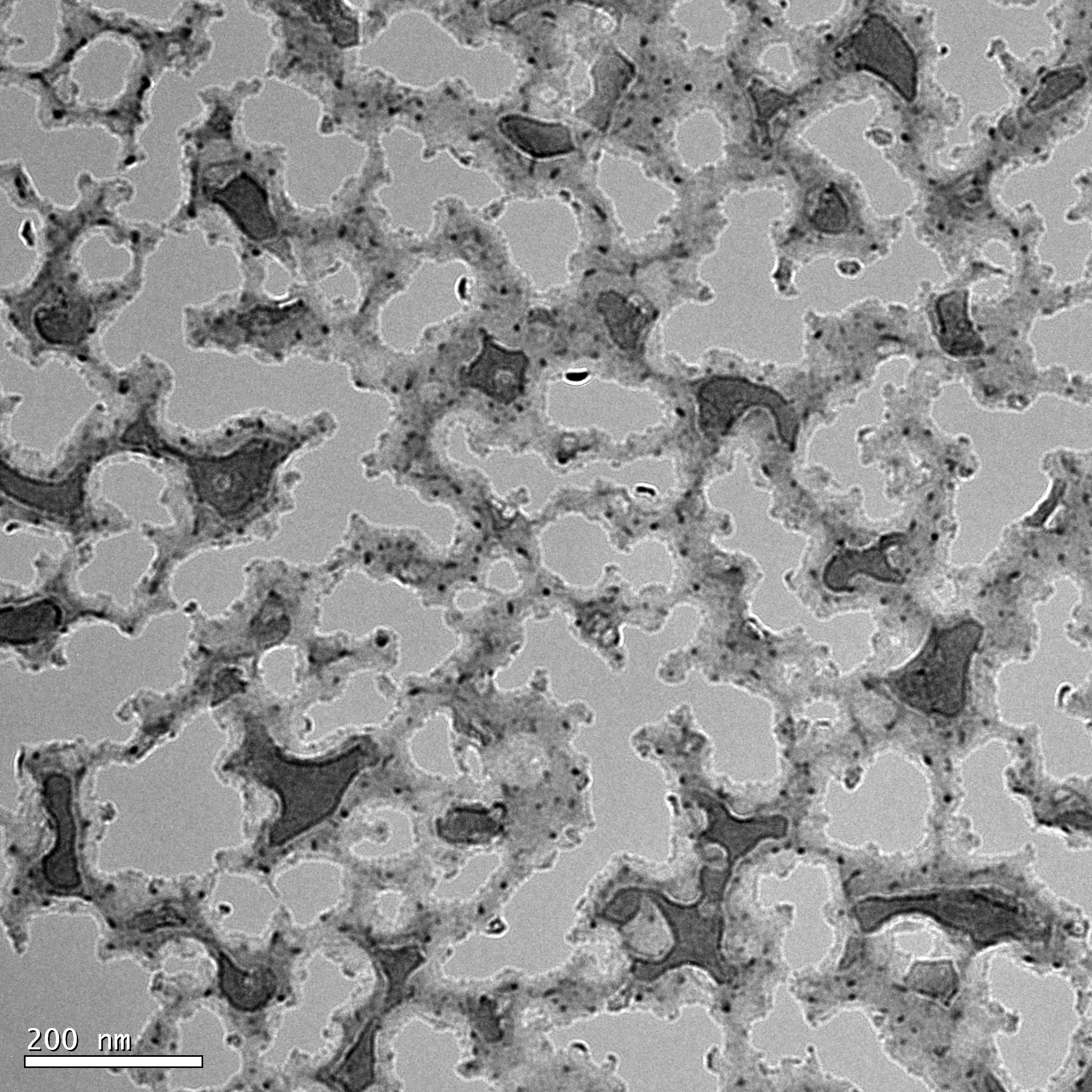
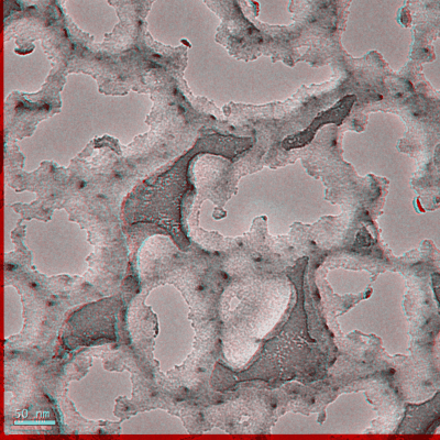
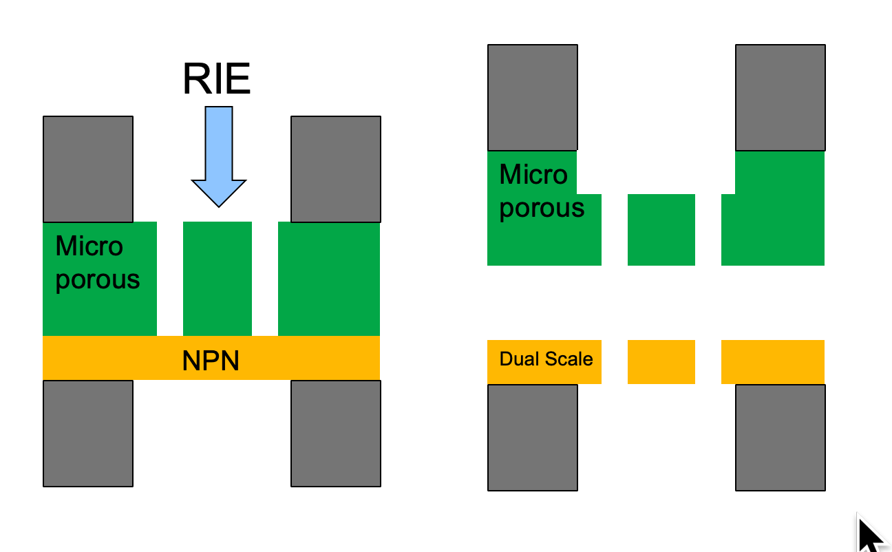
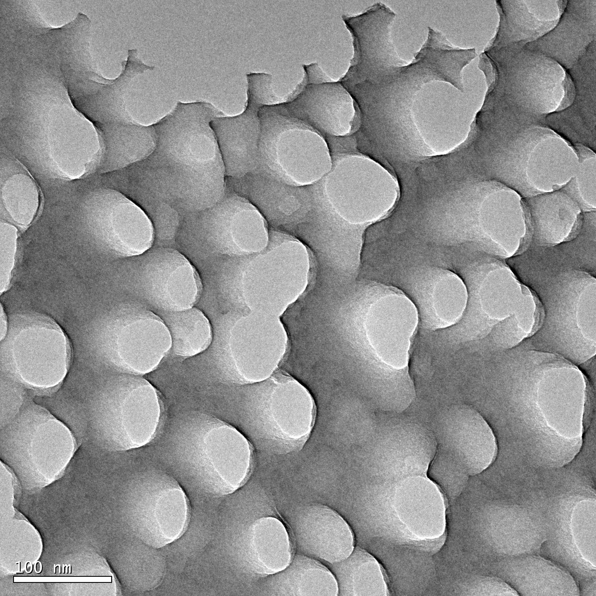
The fabrication of NPN relies on the formation of pnc-Si over a non-porous SiN film, then etching the pattern of the pnc-Si into the SiN. I used the same concept to replicate the dual-scale nanomembrane style (microporous+nanoporous) featured in Alec’s work, as well as create a porous/nonporous nanomembrane substrate, by using existing SiN or NPN chips as shadow masks. Basically, flip a silicon nanomembrane on top of a target substrate, and etch the pattern of the pores into the substrate, using our standard etch process at URnano. Surprisingly, the masking behavior is good to a few microns over the course of etching ~100 nm silicon nanomembranes. Some optimization needs to occur, but this should work well for copying pore patterns in a variety of settings without having to do a lithography process.
Dual-Scale Nanomembrane Procedure
- Clean Etch chamber by using a 100 W Argon Plasma (50 SCCM Ar) for 2 min, then season the etching chamber with standard SF6 recipe (120 sec).
- Take a substrate chip (100 nm NPN) and a microporous masking chip (400 nm thick) and lay the masking chip over the substrate chip
- Alignment done by hand with tweezers. Larger chunks of chips for batch processing should be easier to align.
- Use the standard SF6 recipe to etch into the NPN
- 15 SCCM O2
- 30 SCCM SF6
- 10 SCCM CHF3
- 100 W FWD PWR (0-2 W REF)
- Base Pressure 5e-5 torr (tolerate up to 1e-4 torr)
- 30-50 mTorr Etch Pressure
- Timed etch of 120 sec (this is probably overkill for this process)
- Remove chip stack and gently slide mask off of the substrate chip.
Microporous Transfer into NPN


NPN-Pattern Transfer Procedure
- Clean Etch chamber by using a 100 W Argon Plasma (50 SCCM Ar) for 2 min, then season the etching chamber with standard SF6 recipe (120 sec).
- Take a substrate chip (~50 nm non-porous SiN) and a nanoporous masking chip (100 nm thick) and lay the masking chip over the substrate chip
- Alignment done by hand with tweezers. Larger chunks of chips for batch processing should be easier to align.
- Use the standard SF6 recipe to etch into the NPN
- 15 SCCM O2
- 30 SCCM SF6
- 10 SCCM CHF3
- 100 W FWD PWR (0-2 W REF)
- Base Pressure 5e-5 torr (tolerate up to 1e-4 torr)
- 30-50 mTorr Etch Pressure
- Timed etch of 60-70 sec (this is a very unforgiving process)
- Remove chip stack and gently slide mask off of the substrate chip.
- Some remnants of the masking membrane remain