Strengthening MgF2 nanomembranes through Annealing
In my last post, I described a new process for reducing fluoropolymer build up during RIE. Unfortunately, the new process had substantially lower yields (half) than the process I was using before. In this post, I am detailing my attempts to make the MgF2 nanomembranes stronger to try and improve the yield of my current etching process. I found a paper that discusses the stresses of MgF2, as a function of temperature and film thickness.
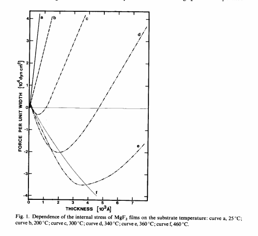
Many industrial references to putting down thin films of MgF2 recommend temperatures of 250C, and from this graph it is apparent that these films result in the most tensile stresses possible (sub 80nm). While I have previously performed depositions at room temperature and at 25oC, I have found that only the 250C deposited films have the mechanical strength to hold up to RIE (room temperature films are more like a dust, than any particular film). In that spirit, I have used 3″ tube furnace in URnano to anneal room temperature deposited films to create more robust films. The tube furnace warms up in a triple temperature zone, so from room temperature, I set the furnace temperature, insert the chips in a ceramic boat, and anneal for 2 hrs. 3 chips were used at each temperature.
500 C – produces easily scratchable films, mechanically indistinct from room temperature films
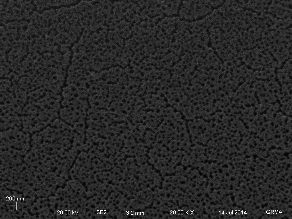
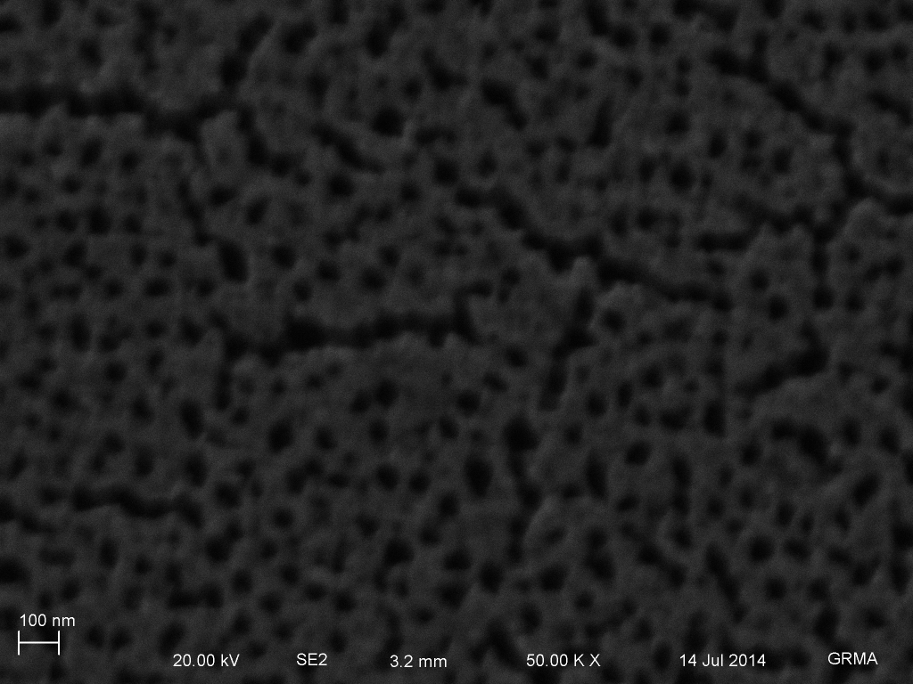
600 C – Films are unbroken, smooth, but are granular under DIC
700 C – Films are unbroken, smooth, non granular under DIC (comparable to 250C deposition)
800 C – Films are unbroken, but have small spiderweb fissures
My initial runs at 250 C in the tube furnace produced annealed films that did not differ at all from the room temperature films. Therefore, I kept increasing the temperature until the mechanical characteristics were similar to that of the films deposited at temperature.
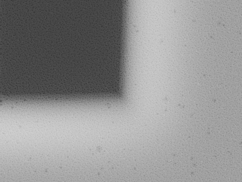
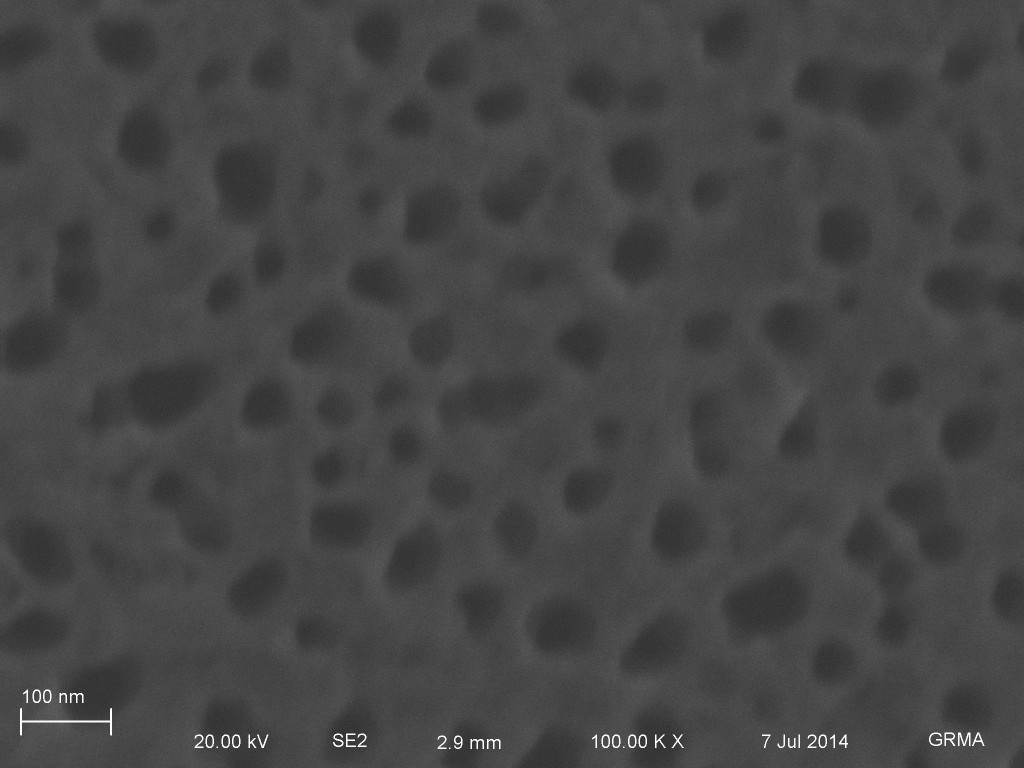
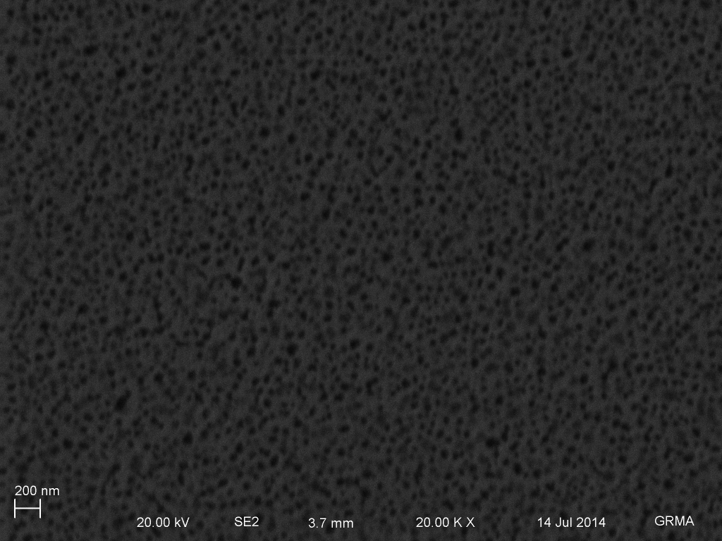
For my experiments, I have been using wafer 1127 (41 nm average pore diameter, 14% porosity, SEPCON format, circular chips)
This process change restored my yield from 15% to about 30% (7/22 at 700C).