Nanopockets membranes for EV’s isolation
Goal:
Is to produce a membrane has pockets to capture the extracellular vesicles EV’s.
Membrane structure:
Figure 1 shows the membrane structure. The membrane will have two pores sides: upper and lower. The pores on top are bigger than the bottom and the diameter of the pores should be similar to or larger than the size of an EV in order to capture them. On the other hand, the bottom pores allow proteins and others to transmit through the membrane and help capture and release the EV’s.

Figure 1: Membrane structure
Method:
Figure (2) shows membrane fabrication process of producing the membrane. Step 1, Positively-charged nanosphere (NS) were attached to the 2 inch wafer. Step 2, the wafer was coated with around 1 um parylene. The parylene thickness should be equal in all wafer. Step 3, the parylene was etched to the half of the NS. Step 4, dissolve the NS. The wafer was sequentially sonicated for 5-10 minutes in toluene, acetone and Iso-propyl alcohol (IPA) respectively.

Figure 2: Membrane fabrication steps
Results:
Step 1: Nanosphere deposition:
The 200nm NS are attached in the wafer in figure 3. It is clear that there are some areas where the NS have aggregated and are more concentrated.

Figure 3: SEM of the NS on the wafer
Step 2: Parylene coating:
Figure 4 shows the 1 um of parylene in top of the 200 nm NS. It is clear that the parylen thickness is not equal in all wafer (see red arrows). To solve this issue, it need to increase the parylene deposition for around 2 um.
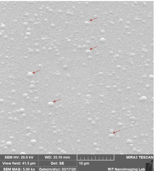
Figure 4: SEM of 1 um of parylene
Step 3: Parylene Etching:
The thickness of the membrane after etching is around 100 nm. It is measured by using Nanometrics NanoSpec. It is clear that the NS are over the membrane (red arrows in figure 5). The etching time is around 55 seconds and the gases used are SF6 and O2
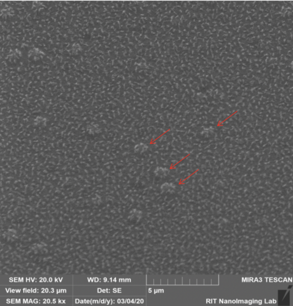
Figure 5: SEM after etched the parylene
Step 4: Dissolving the NS + Loose the membrane:
From figure 6, it is clear that the shape of the membrane is almost same what we plan to fabricate. The upper hole is around 500 nm and the bottom hole is around 100 nm. The holes are larger than expected when considering the amount of time that we etched. Perhaps we etched for too long.
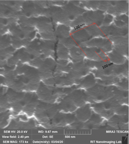
Figure 6: SEM of the membrane after dissolving the NS
Figure 7 shows the backside of the membrane shows small holes around 100 nm (red arrows).
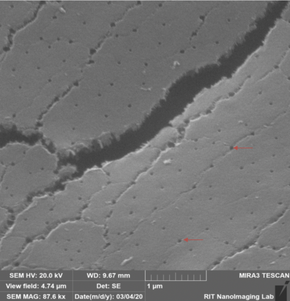
Figure 7: SEM of backside of the membrane
The aim on this membrane is to have the same results as those once obtained Shayan (shown below).

In my opinion, uniformity of coatings over beads is very crucial. For the successful images I got, I had <6 um over 1 um beads and I think it still needed more coating in order to have a smooth surface over beads. When it comes to 300 or 200 nm, I think a very simple experiment would be very helpful. Conduct coatings of 2, 3, 4, and 5 um on 200 nm bead size and without etching, get an SEM image and compare it to Figure 4.
For Figure 3 and distribution of beads, there is still significant agglomeration. In the past, using 10% Sodium dodecyl sulfate (SDS)in the bead solution have shown to help. We certainly can try this after the break. We have it in the lab
Nice post. Are you using micro90 as the sacrificial layer for lifting off of the membranes at the last step (like the rest of our parylene membranes). If yes, is it stable in the bead deposition step (since beads are in a solution) or in the bead dissolving step? if no, what is your alternative method for lift off?
I did not use sacrificial layer. The membrane it has a little bit loose from the wafer by using Toluene, Acetone and IPA (Step 4).